EBSD Analysis Becomes More Accessible with Coxem’s Tabletop SEM
Electron Backscatter Diffraction (EBSD) analysis has seen a surge in popularity among materials scientists and engineers, driven by its capability to provide valuable insights into crystallographic orientation and phase identification. This growth has been further fueled by Coxem’s recent announcement of EBSD capability on their compact, tabletop Scanning Electron Microscope (SEM) models.
Affordable EBSD Solution for Materials Characterization
Traditionally, EBSD analysis has been performed on large, expensive SEM systems, making it inaccessible to many research labs and industrial facilities with limited budgets. Coxem’s innovation brings this powerful technique within reach by integrating EBSD functionality into their cost-effective, benchtop SEM solutions.
Benefits of Tabletop SEM-EBSD Integration
- Reduced Capital Investment: Coxem’s tabletop SEMs with EBSD capability offer a significantly lower upfront cost compared to dedicated EBSD systems.
- Space-Saving Design: The compact footprint of these tabletop SEMs makes them ideal for laboratories with limited space.
- Versatile Materials Analysis: EBSD analysis on Coxem’s SEMs enables comprehensive characterization of metals, ceramics, semiconductors, and composite materials.
With this development, materials scientists and engineers can now perform advanced EBSD analysis at a fraction of the cost, empowering them to gain deeper insights into material properties and optimize their research and development efforts. But with ability to perform EBSD analysis you must also consider sample preparation.
EBSD requires a highly polished, flat surface to be able to get best results. The two most common ways to polish a sample for EBSD are vibratory polishing and ion milling.
Vibratory Polishing
In vibratory polishing, the sample, often mounted in an epoxy “puck”, is delicately polished by the horizontal motion created by the polisher. The vibratory action produces a very flat surface with minimal surface deformation in comparison to a purely mechanical polish from a polishing wheel.
Vibratory polishers are affordable and relatively easy to set up and master.
However, vibratory polishers do not work very well with very small samples that cannot be mounted in pucks. They also require the use of a polishing solution, so are not best if the sample is sensitive to water or oils.
Typical vibratory polishing times run from an hour to several hours.
Ion Milling
In ion milling, the sample is bombarded with ions to remove the top surface of a sample revealing an undamaged area that is clean at the atomic level. Ion milling works under vacuum which keeps the sample clean.
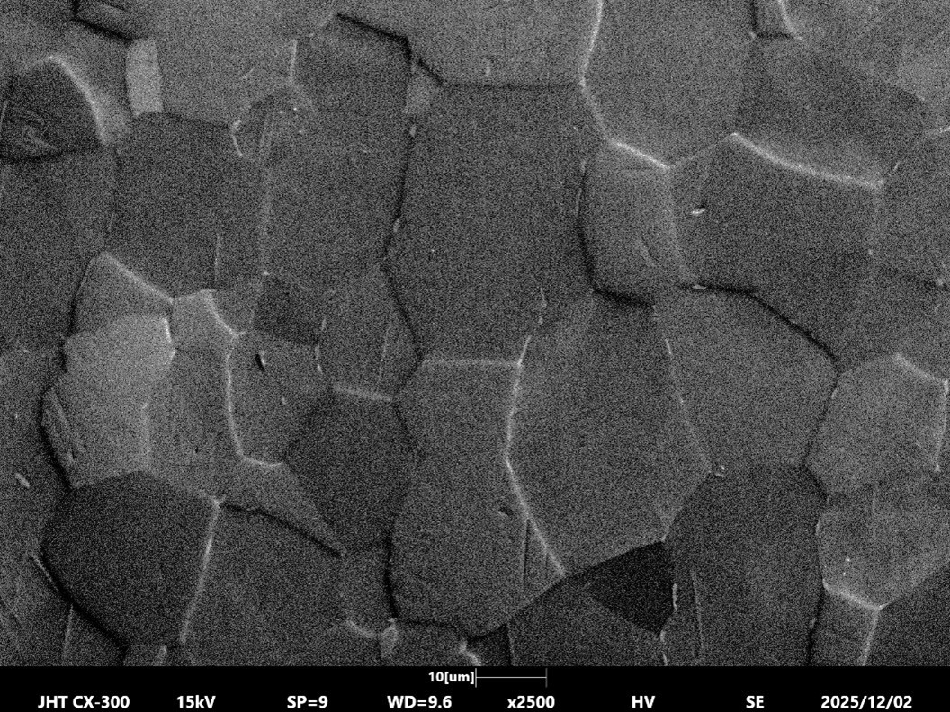
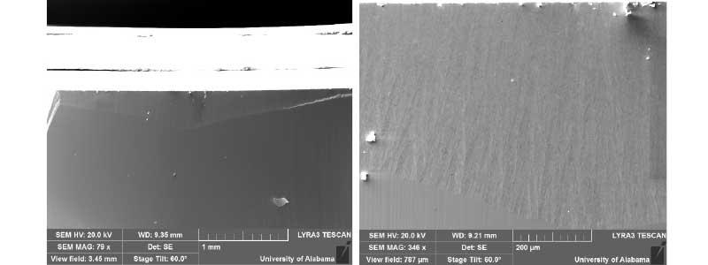
Figure 1: SEM images of the milled steel sample
Which method is better?
The answer is… it depends.
Our lab uses both methods, depending on the material to be analyzed, the size of the sample, and how it is mounted. We find both methods are complimentary in a service lab like ours where samples are so varied.
However, in an environment with minimal variability, you can develop standard processes with a specific polishing tool that makes the most economic sense while providing excellent results.
This example in this application is a steel sample milled on the Leica EM TIC3X ion mill using the cross-sectioning stage. The Leica EM TXP targeting tool was used for sample trimming and polishing down to a 9um, diamond lap. This sample was not mounted in an epoxy puck but mounted directly on a SEM stub.
Figure 1 above shows 2 SEM images of the milled area of the sample. The lower magnification image shows the large milled area that is produced by the TIC3X. The higher magnification image shows the quality of the mill.
There is some topography on the sample that is localized away from the edge of the sample. This is due to the “slope” that builds up in the slope cutting technique as material is displaced from the sample. Despite this topography, EBSD data was successfully collected.
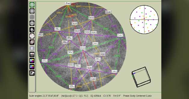
Figure 2: SEM, EBSD map, and typical EBSD diffraction pattern obtained for this sample

Next, two EBSD maps were created for this sample. The first is shown in Figure 2. The left image in Figure 2 shows a nicely polished region in the steel that is nearly free of topography, and grain structure is visible.
The corresponding EBSD map shows clearly defined grains in this region. One of the diffraction patterns is also shown and indexed in Figure 2.
The EBSD system used for this work was set to collect data quickly over a relatively large area. Therefore, individual patterns at each point in the image were collected with relatively low resolution. However, the confidence index for this scan is quite high.
Figure 3: SEM image and EBSD map of the steel sample over a larger area
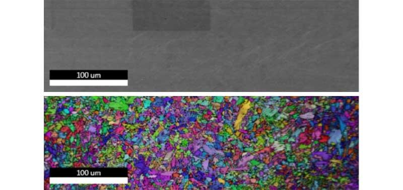
Figure 3 shows an SEM image and corresponding EBSD map for the sample near the first map, however this data covers a much larger area on the sample.
Again, the SEM image shows a region with a very good quality mill that is free of topography. The EBSD shows very clearly defined grains in the steel. Due to the large area, the image does begin to go out of focus on the right side, which explains the blurry appearance on the right side of the image. However, analysis software returned acceptable confidence indices for the patterns obtained to generate this map.
If you have questions or need assistance with your sample preparation process, please use the form on this page to contact us. Or, give us a call at (408) 436-6336.

