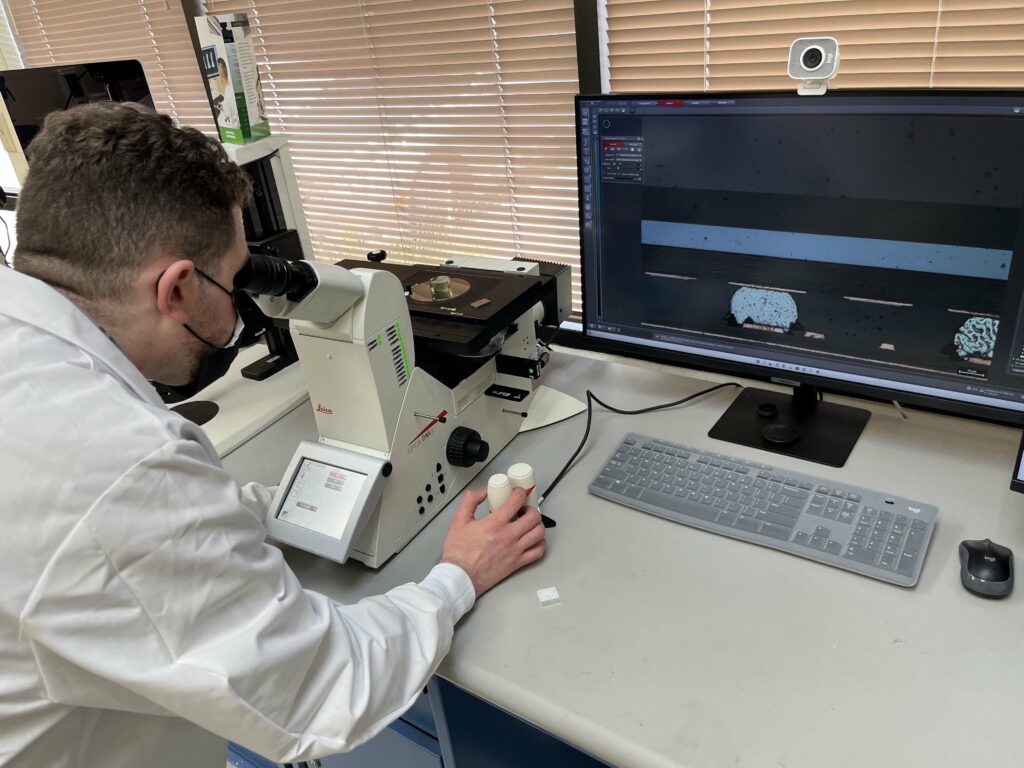
As PCBAs become ubiquitous in our daily lives, manufacturing and assembly houses are under increasing pressure to increase output and maintain razor-thin margins to remain competitive.
The natural consequence of these forces is a drift in quality. Through meticulous analysis, defects, damages, or other anomalies can be rapidly identified and reported so that corrective actions can be taken. Steps may include visual inspection, optical microscopy, X-ray inspection, optical profiling, SEM-EDS, cross-sectioning, and more.
JH Analytical PCB and Component Quality Validation Services
- Dimension and Tolerance Verification
- Flatness Verification
- Optical Microscopy
- Contamination Identification
- X-Ray Inspection and Micro-CT
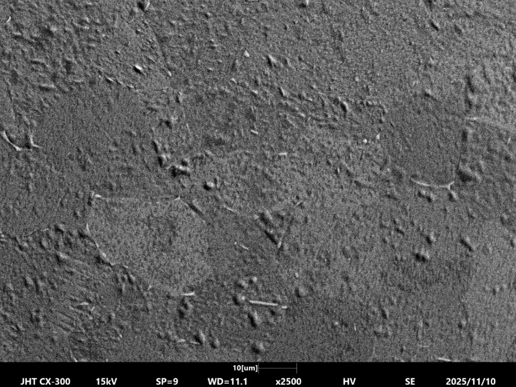
- SEM Inspection
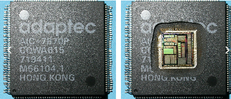
- Mechanical Cross Section
Related PCB and Component Quality Validation
Tools
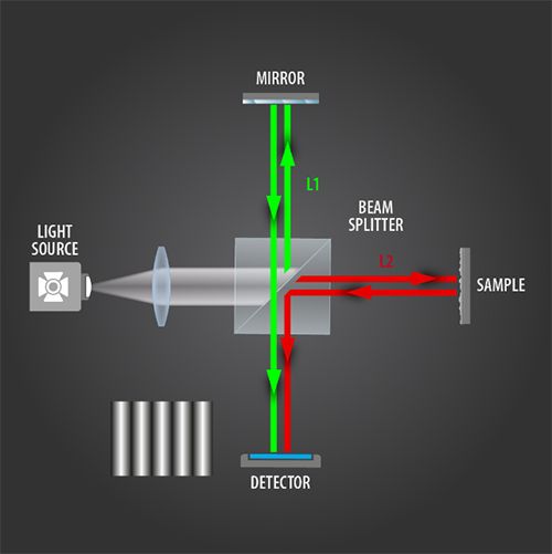
- Sensofar S Neox
- Buehler AutoMet 250
- Buehler EcoMet 30
- Buehler VibroMet 2
- Leica EM TIC 3X
- Leica DM2700M
- Leica DMi8
- ThermoFisher Apreo S Field Emission SEM
- Oxford Ultim Max 100 EDS Detector
- Leica ACE600