Elevating PCB Quality Control: Sensofar’s 3D Metrology Solutions

PCB Quality Control | Sensofar

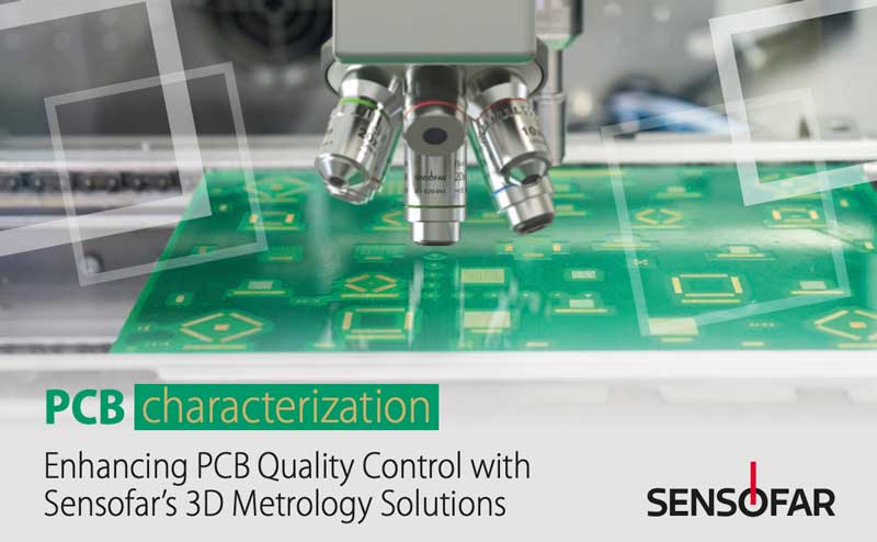
In the realm of advanced electronics manufacturing, the quality and reliability of printed circuit boards (PCBs) are paramount. Each step of PCB production, from copper preparation to components assembly, demands precision and meticulous attention to detail to ensure optimal performance. Sensofar, with over two decades of expertise in 3D optical metrology, presents a comprehensive solution to elevate PCB quality control.

This document delves into the intricate world of PCB characterization, highlighting how Sensofar’s cutting-edge technology empowers manufacturers to enhance quality, streamline processes, and ultimately deliver superior PCBs to the market.
Contact Us

Recent Posts

Unlocking Material Performance with EBSD

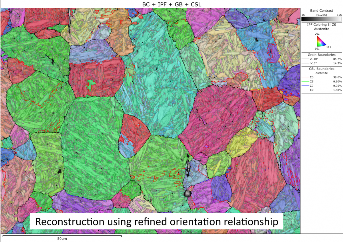
Materials Characterization / Technical Article Electron Backscatter Diffraction (EBSD) Microstructural characterization for failure analysis, process validation, and materials reliability assessment. Author: Tim SchoenRole: Lab Director, JH Technologies Technical contents Summary

Read More »

Chemical Decapsulation

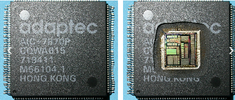
Author Tim Schoen, Lab Director, JH Technologies Access the Die. Preserve the Evidence.   Chemical decapsulation is a controlled sample preparation technique used to remove the plastic encapsulant from semiconductor

Read More »
EDS-chart-with-elements

Elemental Analysis: SEM+EDS

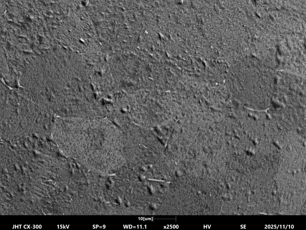
Author Tim Schoen, Lab Director, JH Technologies Understand What Your Material Is Made Of When a contaminant, corrosion site, or unknown particle appears, EDS analysis from JH Technologies helps identify

Read More »

CONTACT US