Metallic materials are fundamental to modern industry, and their performance directly affects product quality and service life. With increasing demands in materials science, there is a growing need to understand the microstructure and elemental composition of metals.
Scanning electron microscopes (SEMs) provide high-resolution surface imaging and utilize spectroscopic techniques , allowing for detailed metal materials observation and elemental analysis. This article outlines how scientists use SEM technology to characterize metal materials and provide insights and guidance for related research.
How SEMs Work
A scanning electron microscope operates by directing a high-energy electron beam at a sample surface. As the high-energy electron beam interacts with the material, it generates various signals, including secondary electrons, backscattered electrons, and characteristic X-rays. Detectors then collect the signals and process them into morphological images or elemental distribution maps of the sample.
Metallic Materials Research—SEM Applications
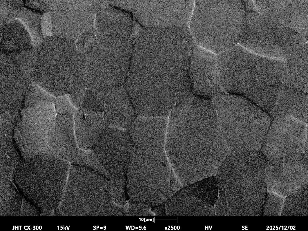
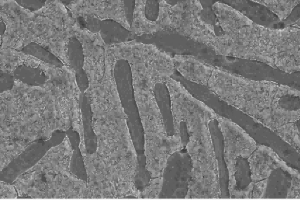
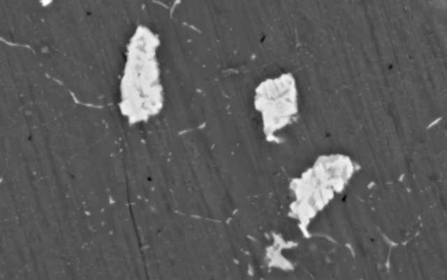
Microstructural Analysis
CIQTEK SEM systems provide high-resolution imaging that enables researchers to analyze key microstructural characteristics of metals and composite materials, including:
- Grain size and shape
- Phase distribution
- Defects such as cracks or inclusions
Understanding these structural features is essential for studying how material properties relate to processing techniques.
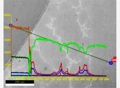
Composition Analysis
When equipped with an energy dispersive spectroscopy (EDS) or wavelength dispersive spectroscopy (WDS), CIQTEK SEMs enable both qualitative and quantitative elemental analysis. This is valuable for:
- Identifying alloying element distribution
- Observing compositional variations
- Understanding how elemental content affects performance
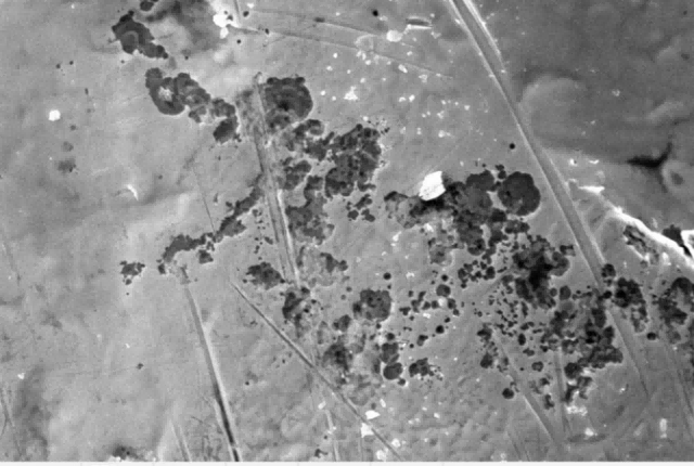
Failure Analysis
After metal materials experience failures such as fractures or corrosion, SEMs can be used to analyze the failure mechanisms. Surface features and corrosion damage are examined to determine the cause, which supports improvements in reliability and service life.
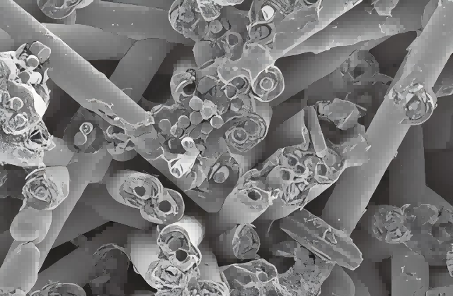
New Material Development
In the development of new materials, SEMs verify the synthesis process and examine structural characteristics. This includes:
- Nanomaterials
- Multilayer films
- Nanocomposites
These observations support research and innovation in materials development.
Interface and Coating Research
The performance of composite materials is closely tied to the quality of interfaces between different phases. SEM imaging allows for the detailed observation of interface characteristics and supports improvements in composite design.
Explore CIQTEK SEM Solutions for Metal Characterization
From microstructure and composition to surface and coating failure analysis, SEM is essential for anyone working with metal materials. CIQTEK’s high-resolution SEM systems—available through JH Technologies—offer the imaging performance and analytical capabilities needed to support today’s most demanding materials research and quality control environments.
Explore our full lineup of CIQTEK scanning electron microscopes to find the right system for your lab, or talk to an expert about your specific application.