In JH Analytical’s latest application note, we explore the science, working principles, and applications of white LED technology. Read on to gain valuable insights into the advancements and potential future developments.
Jump to White LED Lab Analysis
The Rise of Fluorescent Lighting
In 1761, Ebenezer Kinnersley, an English inventor, demonstrated incandescence by passing a current through a single resistive filament. It was likely a short-lived spectacle, producing little visible light and destroying the filament. However, what was perceived as a gimmick at the time, eventually sparked a revolution in electrical lighting.
By 1802, Humphry Davy, a professor at the Royal Institution of Great Britain, had successfully demonstrated what many consider the first light bulb using a high-power electric battery and a thin platinum filament. While dim and impractical, it paved the way for continuous improvements, ultimately leading to the first commercially viable incandescent light bulb patented by Thomas Edison in 1880.
Thanks to its affordability and practicality, the light bulb became one of the first technologies to be adopted by the masses as electrical grids expanded in the early 20th century. Fast forward past the various iterative improvements and scandals (perhaps we’ll cover the Phoebus cartel again) and arrive in 2023. Sitting at my desk, I count over 70 individual light sources. Roughly half are fluorescent, and the other half are LEDs, but not a single fixture is incandescent. So, what happened?
LEDs: The Efficient Light Source
While there were countless improvements in the design of incandescent bulbs, like frosted glass, hermetic housings, argon fill, and wound tungsten filaments, they remained intrinsically inefficient. Even at their peak, household incandescent bulbs only achieved a luminous efficiency of ~2%, meaning most of the power dissipated by the bulb was lost as heat/infrared light. As populations grew more wary of their collective impact on the environment, the inefficiency of the prolific incandescent bulb was thrown into the spotlight.
For a brief period, fluorescent lighting became the de facto efficient light source, touting a 25% improvement in efficiency over the incandescent bulb. As this revolution progressed, the compact fluorescent bulb was mass-produced to accommodate standard household sockets initially designed for incandescent bulbs. Fluorescent bulbs are filled with low-pressure mercury vapor, which emits UV light when excited by an electrical current. This UV light is then absorbed by a fine layer of luminescent white powder called phosphor which lines the inner wall of the glass. Phosphors (not to be confused with phosphorous) have the unique property of absorbing UV light and fluorescing to emit light at lower energies/longer wavelengths. Many different phosphors have been discovered which emit different wavelengths of visible light. Therefore, a combined spectrum of white light can be produced by catering to the ratios of these phosphors.
But, as many of you may have noticed, fluorescent light bulbs are being installed less and less frequently. Enter light-emitting diodes, or LED technology.
What are LEDs?
- LEDs are electroluminescent semiconductor devices that generate light with a p-n junction (called “diode”).
- As voltage is applied across the device, electrons, and holes recombine at the p-n junction/depletion region and produce photons/light.
Analysis of White LEDs
Early commercially available LEDs emitted invisible infrared light at low intensities, limiting their use to products like remote controls. As advancements were made in semiconductors and novel materials were introduced, LEDs became available in visible wavelengths and UV. An apparent white light could be formed by combining red, green, and blue LEDs (much like the monitor you are likely reading from right now). While this method is viable for products like monitors, it requires the inclusion of 3 separate LEDs in red, green, and blue. So how do we produce white light from a single LED?
Fortunately, a well-documented set of materials already exists that can convert UV light into visible white light – phosphors! Nearly all white LEDs in modern products like flashlights and cell phones utilize photoluminescent phosphors. Gallium nitride (GaN) is the semiconducting material for mass-producing UV LEDs.
White LED Lab Analysis: Internal Components
For this month’s application note, we analyzed white LED technology from a 5-year-old phone graciously donated by one of our employees. We will not detail the specific make or model out of respect for the manufacturer (and in an abundance of caution).
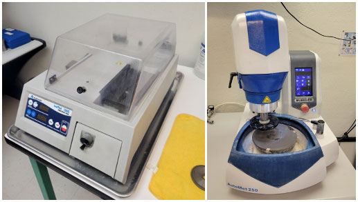
We disassembled the phone and separated its internal components until we were able to extract the LED board. Next, we secured the board with a specimen clip and encapsulated it in Buehler EpoKwick fast-cure 2-part epoxy resin puck. Once fully cured, we trimmed the puck with a Buehler IsoMet 1000 Precision Cutter and then mounted and polished it using a single force specimen holder on a Buehler AutoMet 250.
Sample Polishing Challenges for White LEDs
In modern white LED technology, the phosphor material is suspended in soft silicone to minimize the absorption of both UV and visible light. However, the contrasting hardness of the GaN and silicone make it difficult to polish the sample because the GaN die is exceptionally fragile at only 5µm thick. Therefore, we reduced the polishing force to mitigate the rounding of the die, in addition to testing various silicon carbide, alumina, and diamond media were tested to determine the optimal polishing conditions.
A Smooth LED Sample for Ion Beam Milling
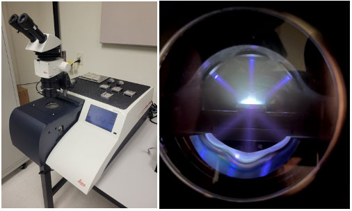
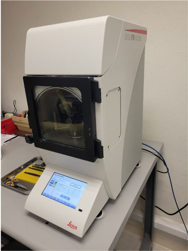
With the sample surface visibly smooth, we then transferred the puck to a Leica EM TIC 3X ion beam milling system and flat-milled it to remove any final surface imperfections. This tool utilizes three independent de-focused ion guns covering a larger area than most ion mills in conjunction with stage translation and rotation. This lesser concentrated ion bombardment permits low-power milling of sensitive organics like silicone and epoxy without the need for a cryo-stage.
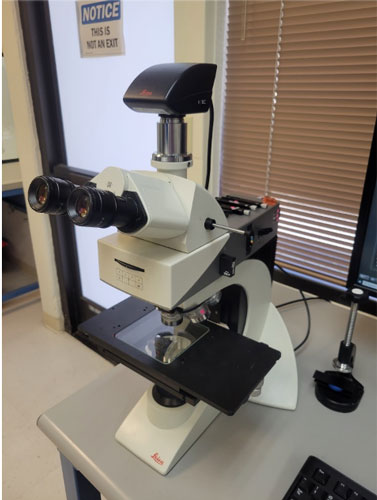
After flat milling, we inspected the sample and performed imaging using a Leica DM2700 M compound microscope with a Leica K5C 20MP CMOS camera.
Anatomy and Function of the LED Board
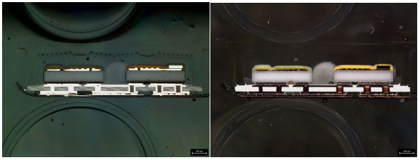
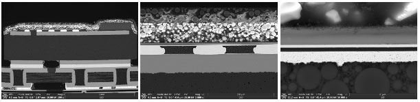
The board had two mounted LEDs mounted, each with a unique coloration to the silicone/phosphor layer. Each LED emits light of a specific “temperature” of white light. One is “warmer” (more orange/red), and the other is “cooler” (more blue), allowing the temperature of the flash to be fine-tuned when taking photos by assessing the local lighting with the camera and adjusting as needed to provide a neutral tone. On top of the phosphor layer, we see a white diffusion layer.
At the top of the package, we see a transparent polymer structure with ridges symmetrical about the centerline. This structure is essentially two Fresnel lenses side by side. Fresnel lenses are lightweight and low-mass alternatives to full-size lenses, and they are well suited to applications with diffuse light where ridges in the lens do not impact the overall function.
The Next Step: Sputter Coating
Next, we coated the LEDs with a 10nm thick AuPd film using a Leica EM ACE600 high vacuum sputter coater and imaged them using an SEM.
The die and substrate are gold-plated and secured with a grid of gold ball bonds. The GaN die itself is extremely thin at only ~5µm. GaN has a Wurtzite/hexagonal crystal structure that lends itself more readily to epitaxial growth. Hence GaN devices are often grown on other substrates like Si or sapphire. Sapphire substrates can be patterned to optimize light output, but silicon substrates tend to absorb emitted light, so they are often removed, leaving only the thin epitaxially grown GaN layer. This LED is utilized as a flip chip, meaning there is no metallization on top of the die to interfere with the light output. The thinner die helps to minimize the absorption of UV photons from the depletion region as they travel through the GaN to the exposed die surface and into the phosphor layer.
EDS Reveals the Composition of LED Materials
Next, we collected energy-dispersive x-ray spectroscopy (EDS) maps to determine the composition of the various LED materials.
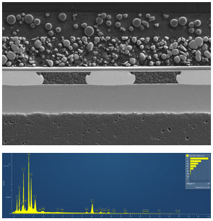
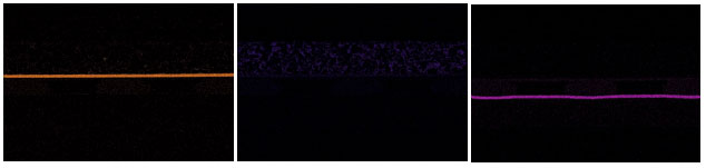
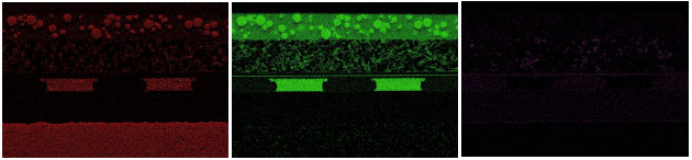
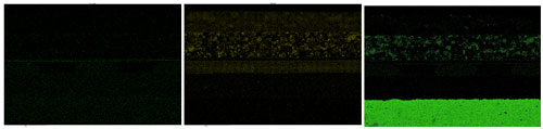
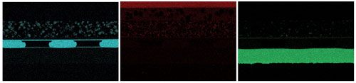
The particles within the phosphor layer contain yttrium, aluminum, and oxygen, indicating a YAG:Ce phosphor. Yttrium aluminum garnet (YAG:Ce or Y3Al5O12) doped with Cerium far below the lower detection limit of EDS. The diffusion layer over the phosphor contains silicon dioxide (glass) beads within an organic film. The die metallization comprises at least three unique layers: titanium (possibly a TiN barrier metal), silver, and gold. Over the alumina substrate, we see what appears to be a standard ENIG (electroless nickel and immersion gold) over copper. However, any phosphorous signal typically associated with electroless nickel is masked by the peaks at the lower end of the spectrum.
Efficiency and Future of White LED Technology
The sheer complexity of the modern LED compared to the long-lived filament light bulb is a testament to the increasing pace of technological progress. With an efficiency of around 75%, it’s clear why white phosphor LEDs are regarded as the future–they represent a massive leap in efficiency that is directly tied to improved battery life for handheld devices, reduced bills for households and businesses, and a reduced carbon footprint for generating our electricity. It should be noted that, depending on the composition, the phosphor layer has a conversion efficiency of 80-95% – the underlying LED is even more efficient than the stated 75%.
Expectations for Continued Innovation in LED Lighting
As long as investment in semiconductor research remains strong, we can expect continued innovation in LED lighting. Increasing efficiency and decreasing costs stand to further fuel demand until, one day, you might look around your office and see nothing but LED lighting. Or maybe, you will see a mix of LED fixtures and the next undiscovered technological breakthrough in lighting. One thing is for sure, the future is not only bright but efficient as well.
Need help with Sample Testing for your application?
Complete the form on this page or contact us.