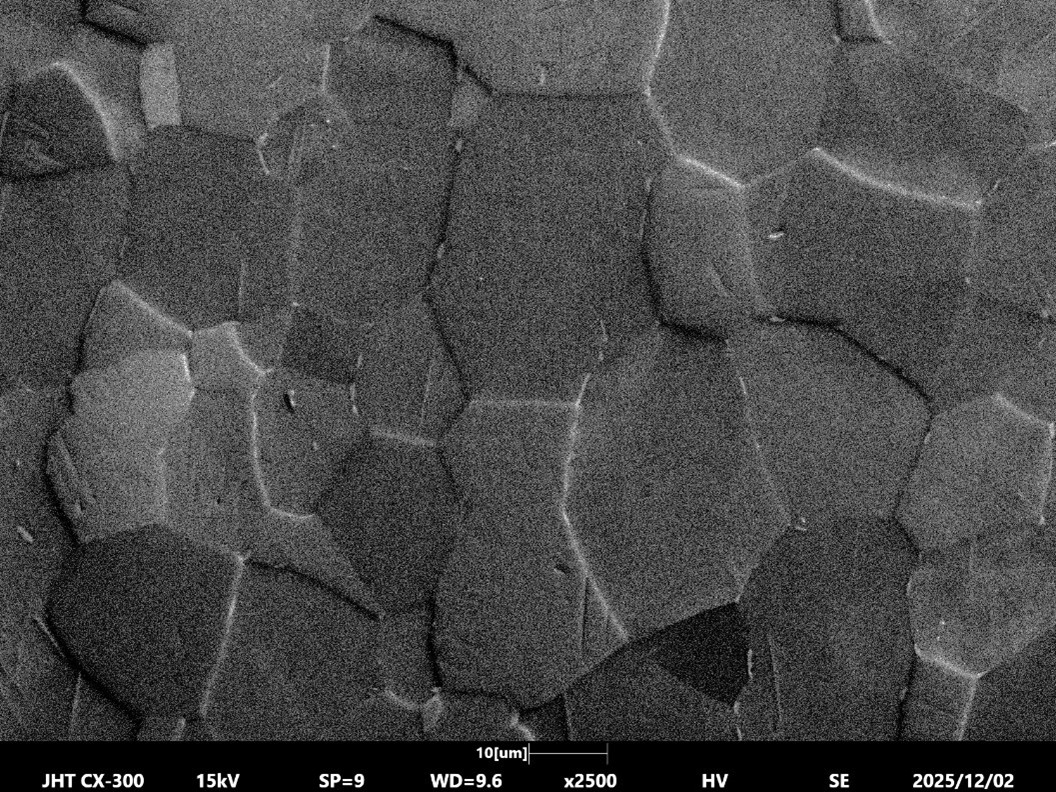
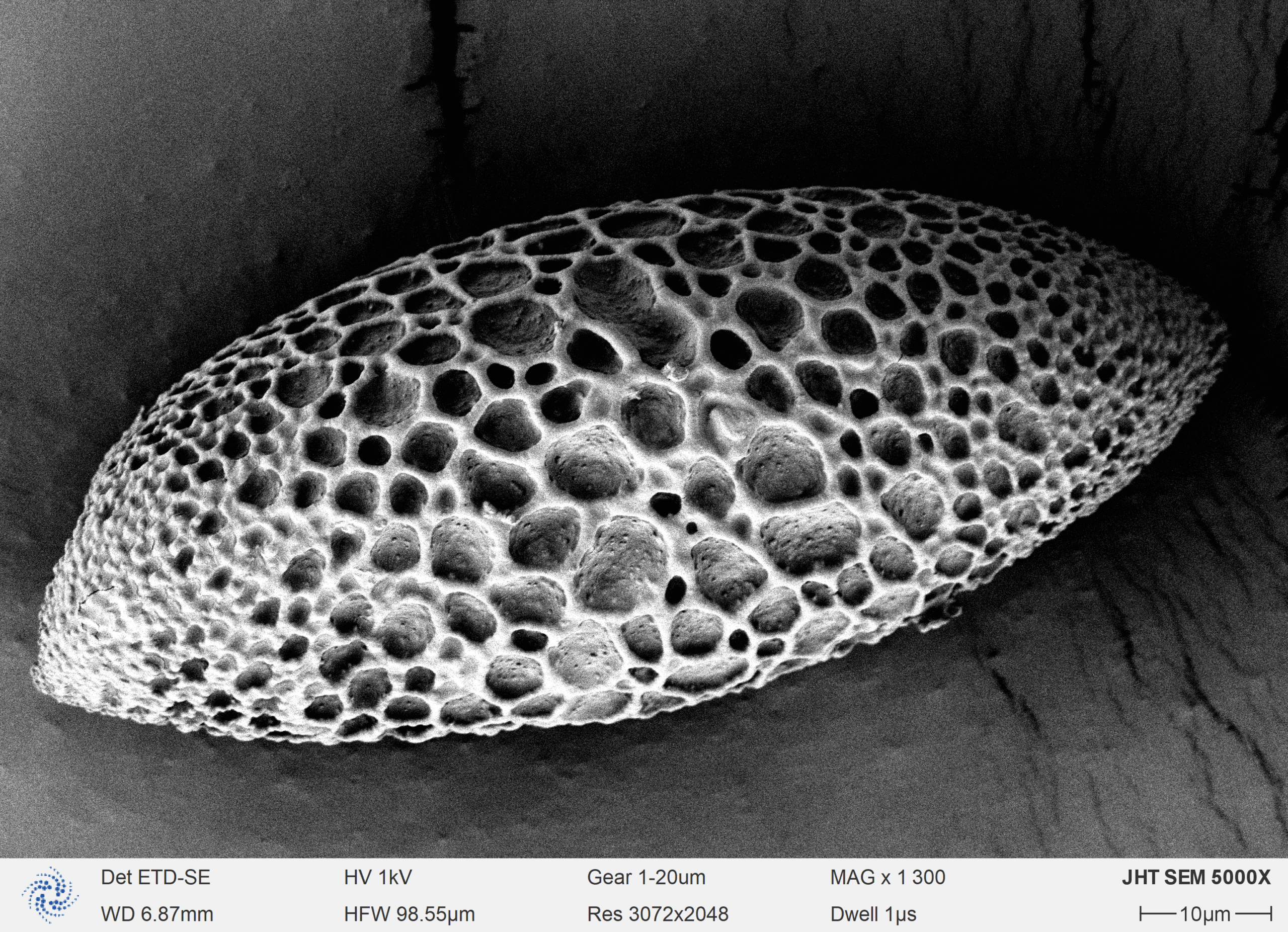
Non-conductive samples often have a charging effect from electrons collecting on the sample surface, causing issues with SEM imaging. While many SEM systems have a “low vacuum” or “charge reduction” mode that can overcome this issue, it usually has limitations in magnification and image quality that is sample-dependent. In addition, images collected in “low vacuum” modes typically have a flat contrast, resulting in unappealing photos.
For the best imaging, we recommend coating non-conductive samples using a sputter coater to apply a nano-thin layer of conductive metal. Even conductive samples benefit from a sputter-coated layer of highly electron-emitting materials like gold, platinum, or gold/palladium. This coating allows imaging at higher beam energies to obtain the highest resolution and magnification without concern for electron charge effects or beam damage to sensitive samples.
Energy Dispersive Spectroscopy (EDS) analysis, along with software, allow you to define the coating metal. You must select a metal coating type that is not present in the sample. Alternately, for the most precise EDS analysis, a carbon coater can be used to produce an x-ray transparent conductive coating. Carbon coating is popular in the mineralogical analysis of resin-mounted, polished samples, and slide-mounted polished thin sections.
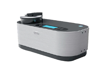
We offer multiple choices for sample coating with metals, carbon, or both. The economical SPT-20 coater is an ideal entry-level coater, best suited for flat samples. The more advanced DESK series coaters are available in low- and high-vacuum models. Since the vacuum level plays a role in the resulting grain size, Field Emission or FE-SEM and TEM use high vacuum coaters to produce images above 100,000X magnification where the potential exists to observe the artifact of coating grains. We can also use high vacuum coating with oxidizing metals like Chrome.
We suggest Echlin’s Handbook Sample Preparation for SEM and EDS for further reading about sample preparation and sputter coating. An online version is also available HERE.
Thermal Evaporation
We offer multiple choices for applying thin films to samples using thermal evaporation, sputtering, or a combination of both. Sputter coating uses a “target” of pure metal, but a thermal evaporator utilizes multiple sources, allowing it to create alloys of different metals in the film. Likewise, through the coater’s control panel, we can perform sequential coating using evaporation or sputtering, depending on the coater’s configuration.
Thermal evaporation is a method of physical vapor deposition (PVD) and typically uses a resistive heat source to evaporate a solid material in a vacuum environment to form a thin film. The coating material is often contained in a “boat,” “basket,” or “coil” made of materials capable of withstanding temperatures higher than evaporated material. The materials to be applied with thermal evaporation techniques can be pure atomic elements, including metals, non-metals, or molecules such as oxides and nitrides. The material is heated in a high vacuum chamber until it produces vapor and coats a substrate.
A very nice summary of published work is available HERE at Science Direct for further reading about thermal evaporation for thin films and coating deposition.
Need help with your lab application?
Complete the form on this page or contact us.