Author Tim Schoen, Lab Director, JH Technologies
A proven, cost-effective technique for identifying failure mechanisms in BGA, CSP, and other advanced electronic assemblies.
Why Dye & Pull Analysis Matters
As electronic assemblies become smaller and more densely packaged, determining the root cause of intermittent electrical failures can be difficult. Solder joint defects, BGA attachment issues, package delamination, and assembly-induced stresses often occur beneath component packages where they cannot be directly observed.

Dye & Pull analysis helps identify where interconnect failures occurred and provides evidence of the failure mechanism. When combined with X-ray inspection, cross-sectioning, scanning electron microscopy (SEM), and energy dispersive spectroscopy (EDS), it becomes a valuable part of a comprehensive failure analysis workflow
This overview explains how the technique works, the types of defects it can reveal, applicable industry standards, and how it fits into a broader root cause investigation.
Hidden Failures Can Be Difficult to Diagnose
Electronic assemblies are exposed to thermal cycling, vibration, mechanical shock, and environmental stresses throughout their service life. These conditions can contribute to failures that are not readily visible during routine inspection.
Common failure mechanisms include:
- BGA solder joint cracking
- Cold solder joints
- Head-in-pillow defects
- Pad cratering
- Intermetallic separation
- Package delamination
- Assembly process defects
Many of these conditions can remain hidden when using traditional inspection methods alone, making Dye & Pull a useful diagnostic tool during failure investigations.
How Dye & Pull Reveals Hidden Defects
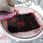
Dye & Pull is a destructive analytical technique used to identify cracking or separation beneath electronic components. The process includes:
- Applying a low-viscosity penetrant dye
- Allowing the dye to infiltrate cracks and voids
- Removing excess dye
- Mechanically separating the component from the PCB
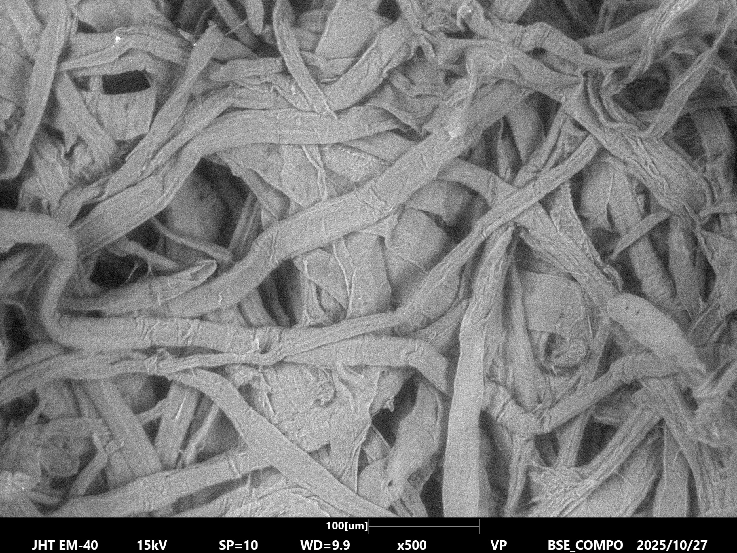
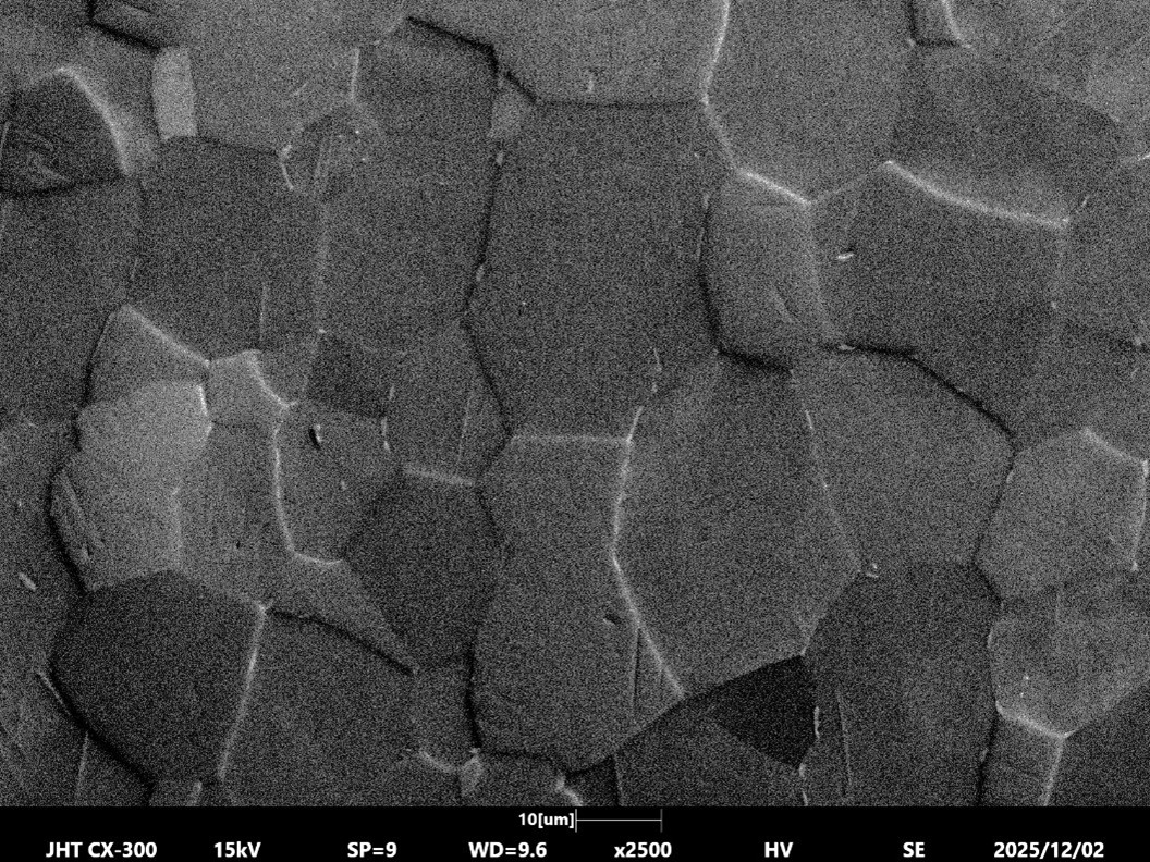
- Examining fracture surfaces using optical microscopy and SEM
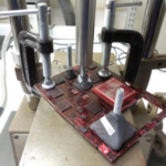
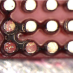
Areas where dye is present indicate locations where a crack or separation existed prior to component removal, providing evidence of the original failure condition rather than damage introduced during analysis.
Results Supported by Industry Standards
Our Dye & Pull analysis is performed in accordance with:
- IPC-TM-650 Method 2.4.53
- Customer-specific qualification standards
- Automotive and aerospace reliability protocols
This provides a documented and repeatable approach suitable for engineering investigations, supplier evaluations, and corrective action activities.
Common Failure Mechanisms Identified
BGA Solder Joint Cracking
Thermal fatigue and mechanical stress can create cracks within solder joints.
Typical indicators include:
- Corner ball failures
- Partial crack propagation
- Complete joint separation
Head-in-Pillow Defects
- Occurs when solder paste and BGA balls fail to properly coalesce during reflow.
- Dye penetration often clearly identifies incomplete solder wetting.
Pad Cratering
Mechanical loading and board flexure can cause cracking beneath PCB pads, resulting in intermittent or permanent electrical failures.
- Dye & Pull analysis helps distinguish pad cratering from solder joint failure.
Delamination
Interface separation between materials may occur due to:
- Moisture exposure
- Thermal cycling
- Manufacturing defects
What to Expect During Analysis
- Failure review and application discussion
- Visual inspection
- X-ray analysis
- Dye application
- Dye curing
- Mechanical separation
- Optical microscopy examination
- SEM imaging
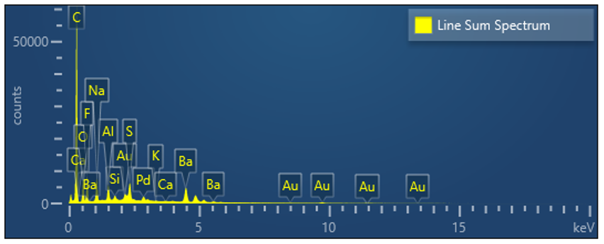
- EDS analysis (when required)
- Failure mechanism determination and reporting
When Dye & Pull Is Most Effective
- Hidden interconnect failures beneath component packages
- Intermittent electrical opens
- BGA and CSP reliability concerns
- Supplier quality issues
- Field returns and warranty failures
- Qualification and reliability testing programs
Additional advantages include:
- Cost-effective compared with more extensive destructive analysis methods
- Provides direct visual evidence of crack locations
- Complements X-ray, SEM, and cross-section analysis
- Supports root cause investigations and corrective action efforts
- Applicable to a wide range of package technologies
Because Dye & Pull is a destructive technique, it is often used alongside non-destructive methods such as X-ray inspection and followed by SEM characterization when additional detail is required.
Integrated Failure Analysis Capabilities
Dye & Pull analysis is most effective when used as part of a broader failure analysis strategy.
JH Technologies can integrate findings with:
- X-ray inspection
- Cross-section analysis
- Scanning electron microscopy (SEM)
- Energy dispersive spectroscopy (EDS)
Combining multiple analytical techniques helps correlate physical evidence with manufacturing history, reliability testing, and field performance to develop a more complete understanding of failure mechanisms.
Real Results From the Lab
Case Study 1: Intermittent BGA Failure
- Customer complaint: Intermittent electrical opens during thermal cycling.
- Findings: Dye & Pull revealed corner-ball cracking on multiple solder joints.
- Root cause: CTE mismatch combined with insufficient solder joint stand-off height.
- Outcome: The customer used our findings to revise stand-off height requirements and prevent recurrence in future production runs.
Case Study 2: Field Return Investigation
- Customer complaint: Product failures after drop testing.
- Findings: Pad cratering identified beneath BGA package.
- Root cause: Excessive mechanical shock combined with PCB design limitations.
- Outcome: Findings informed a PCB design change that improved shock resistance ahead of the next product revision.
Best Practices for Effective Analysis
- Bring Dye & Pull in early in the investigation process
- Combine with X-ray imaging before any destructive analysis
- Thoroughly documenting fracture surfaces
- Using SEM imaging for detailed crack characterization
- Correlate findings with manufacturing history and reliability data
JH Analytical Lab Service
Dye & Pull analysis is one component of our comprehensive failure analysis offering for electronics manufacturers, OEMs, and contract assemblers.
Whether the objective is investigating field returns, evaluating reliability concerns, supporting supplier corrective actions, or qualifying new assemblies, our laboratory combines analytical tools with practical engineering expertise to identify and document failure mechanisms.
JH Analytical Lab Service includes:
- Dye & Pull analysis
- X-ray inspection
- Cross-section analysis
- Scanning electron microscopy (SEM)
- Energy dispersive spectroscopy (EDS)
- Failure review, root cause reporting, and corrective action support
[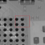 BGA 2D X-ray
 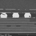 SEM Image
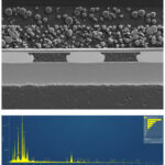 SEM w/EDS
From initial consultation through final reporting, our goal is to provide clear, standards-based findings that help engineering and quality teams make informed decisions.
Discuss Your Failure Analysis Requirements
Dye & Pull remains a valuable technique for identifying hidden interconnect failures in modern electronic assemblies. When integrated with complementary analytical methods, it can provide critical insight into solder joint integrity, package reliability, and failure mechanisms that are otherwise difficult to detect.
If you are investigating intermittent failures, field returns, qualification issues, or reliability concerns, JH Technologies can help determine the most appropriate analytical approach and provide the supporting data needed for effective root cause analysis.