Author Tim Schoen, Lab Director, JH Technologies
Understand What Your Material Is Made Of
When a contaminant, corrosion site, or unknown particle appears, EDS analysis from JH Technologies helps identify its elemental composition and provides data that can support root-cause investigations.
In manufacturing, quality assurance, and failure analysis, a common question is: What is this material?
Contamination, corrosion, coating defects, inclusions, foreign particles, and material substitutions often originate from differences in material composition. Visual inspection alone may not provide enough information. Energy Dispersive Spectroscopy (EDS), integrated with Scanning Electron Microscopy (SEM), identifies the elements present in metals, polymers, ceramics, electronics, and advanced composites, helping engineers and scientists make informed decisions.
What EDS Can Tell You
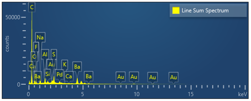
When the SEM electron beam interacts with a sample, it generates characteristic X-rays. EDS measures those X-rays to identify the elements present, adding compositional information to SEM imaging.
EDS can provide:
- Identification of elements present in a particle, residue, or failure site
- Relative elemental concentrations across a region
- Elemental distribution over a surface
- Chemical differences between adjacent areas
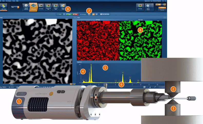
Four Ways We Analyze Your Sample
Every investigation has different requirements. Our applications scientists select the analysis approach based on the question being addressed.
Point Analysis
Composition at a specific location, useful for identifying particles, inclusions, failure sites, and verifying alloy composition.
Area Analysis
Average composition across a selected region for bulk characterization, coating evaluation, and process verification.
Line Scans
Elemental variation across a feature, commonly used for diffusion studies, coating thickness measurements, and interface analysis.
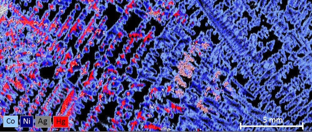
Elemental Mapping
Visual representation of elemental distribution across a surface, often used in corrosion studies, failure analysis, and materials development.
Where EDS Solves Real Problems: Common Applications
Failure Analysis
EDS helps identify the elemental signatures associated with corrosion, fractures, electronic component failures, and material degradation.
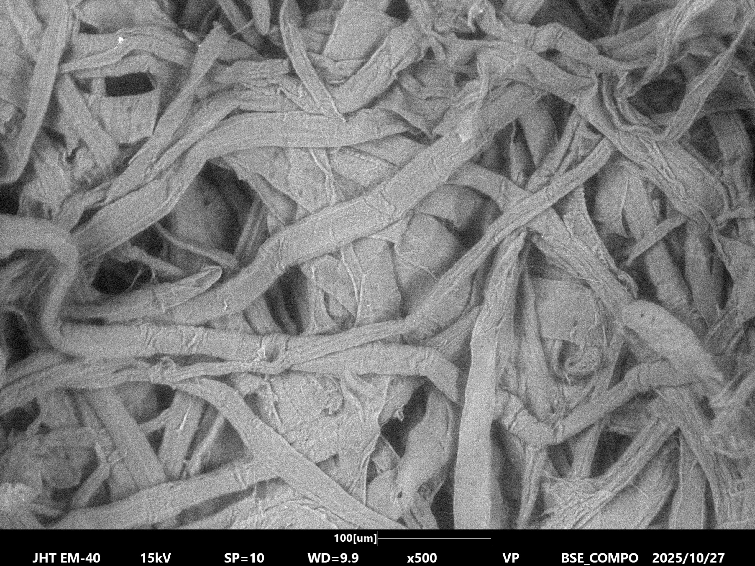
Contamination & Particle Identification
Unknown particles and residues can be analyzed to distinguish process residues, environmental contaminants, metal debris, and other sources of contamination.
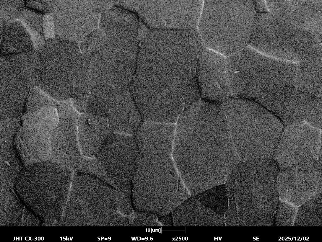
Corrosion Investigations
EDS can detect chlorides, sulfur compounds, oxides, and other corrosion-related species that help determine contributing environmental or process factors.
Alloy Verification
Supports incoming inspection, supplier qualification, counterfeit investigations, and routine quality-control checks.
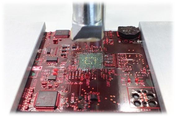
Semiconductor & Electronics Analysis
Used to investigate solder joints, bond wires, package contamination, and elemental variations associated with manufacturing defects or field failures.
Examples from the Lab
Case Study 1: Premature Corrosion on Stainless Steel
- Customer challenge: Stainless steel components were corroding earlier than expected.
- EDS findings: Elevated chlorine concentrations were detected within corrosion sites.
- Conclusion: Exposure to chloride-containing cleaning chemicals contributed to the corrosion
Case Study 2: Foreign Particles Causing Cosmetic Defects
- Customer challenge: Unexplained particles were affecting surface appearance.
- EDS findings: Particle composition matched a worn tooling component.
- Conclusion: Tool wear was introducing contamination during production.
Case Study 3: Intermittent PCB Electrical Failures
- Customer challenge: PCB assembly experienced intermittent electrical failures.
EDS findings: Localized oxidation and contamination were identified on solder joints.
- Conclusion: Contamination introduced during assembly contributed to the failures.
A Complete Analytical Approach
EDS is often most effective when combined with complementary techniques. Depending on the application, investigations may include:
- Visual inspection and optical microscopy
- SEM imaging for structural characterization
- EDS for elemental analysis
- Cross-sectioning and additional analytical techniques as needed
- Data interpretation to support root-cause analysis
Why Work With JH Technologies
EDS is a versatile analytical technique, but meaningful results depend on both data quality and interpretation. Our applications scientists combine elemental analysis with microscopy observations and can recommend complementary methods when additional information is needed. With demonstration centers, an analytical laboratory, and decades of microscopy experience, JH Technologies provides practical analytical support for materials characterization and failure investigations.
- Speed: Rapid elemental analysis that can quickly narrow potential causes and guide further investigation.
- Breadth: Analysis of metals, polymers, ceramics, electronics, and composite materials on a single platform.
- Expertise: Factory-trained applications scientists experienced in microscopy and materials characterization.
- Complete Workflow: Access to SEM, EDS, EBSD, sample preparation, and cross-sectioning capabilities in one location.