Author Tim Schoen, Lab Director, JH Technologies
Access the Die. Preserve the Evidence.
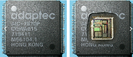
Chemical decapsulation is a controlled sample preparation technique used to remove the plastic encapsulant from semiconductor devices while preserving the underlying die, bond wires, bond pads, and lead frame. The process provides direct access to internal device structures for subsequent inspection and analytical testing.
At JH Analytical Services, chemical decapsulation is routinely performed as part of failure analysis, reliability investigations, counterfeit detection, and process verification. When combined with optical microscopy, scanning electron microscopy (SEM), energy dispersive spectroscopy (EDS), electrical characterization, and other analytical techniques, decapsulation provides the physical evidence needed to identify failure mechanisms and document root cause.
Die-Level Access | Multi-Technique Analysis | Defensible Results |
Exposes the silicon die and package interconnects while preserving critical features for analysis. | Compatible with optical microscopy, SEM, EDS, probing, and additional analytical methods. | Generates documented evidence to support failure analysis, qualification testing, and supplier investigations. |
Why Chemical Decapsulation Is Performed
Many semiconductor failure mechanisms originate beneath the package and cannot be evaluated through external inspection alone. Mold compound obscures the structures responsible for electrical performance, making controlled package removal an essential step in many investigations.
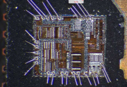
Chemical decapsulation enables direct examination of:
- Silicon die surfaces
- Bond pads
- Wire bonds
- Lead frames
- Die attach regions
- Package interfaces
Access to these structures allows analysts to evaluate damage resulting from electrical, mechanical, thermal, environmental, or manufacturing-related mechanisms while minimizing disturbance to the original failure condition.
Following decapsulation, analysts can:
- Locate die-level failure sites
- Evaluate wire bond integrity and intermetallic formation
- Examine corrosion and contamination
- Identify moisture-related degradation
- Characterize ESD and electrical overstress (EOS) damage
- Verify die identity and manufacturer markings
- Support reverse engineering and authenticity verification
- Prepare devices for SEM, EDS, and additional analytical techniques
Typical Applications
Failure Analysis
Chemical decapsulation provides direct access to failure sites for determining the physical mechanism responsible for field returns, production failures, or qualification issues.
Typical investigations include:
- Electrostatic discharge (ESD)
- Electrical overstress (EOS)
- Bond wire failures
- Metallization damage
- Corrosion
- Die cracking
- Passivation defects
Reliability Evaluation
Decapsulation is commonly performed following environmental or accelerated life testing to determine how stress conditions affected the device.
Examples include:
- Thermal cycling
- Burn-in testing
- HAST
- THB testing
- Power cycling
- Long-term aging studies
Counterfeit Detection
Exposed die markings and internal construction can be compared against known authentic devices.
Common evaluations include:
- Die markings
- Manufacturer identification
- Die dimensions
- Wire bond configuration
- Package construction
- Evidence of resurfacing or remarking
Manufacturing Process Verification
Chemical decapsulation can also be used during process development and quality investigations to verify internal package construction.
Typical inspections include:
- Wire bond placement
- Bond quality
- Die placement accuracy
- Package consistency
- Internal assembly workmanship
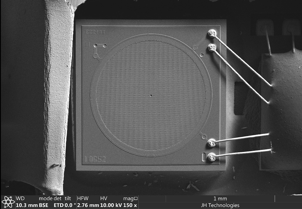
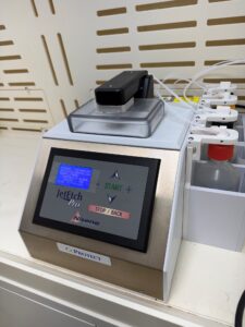
Decapsulation Process
Successful decapsulation depends on maintaining controlled removal of the encapsulant while minimizing attack on the exposed device structures. Process parameters are selected based on package materials, die size, and analytical objectives.
1) Sample Evaluation – Each device is reviewed to determine:
- Package construction
- Encapsulant type
- Sensitive internal structures
- Required exposure area
- Downstream analytical methods
2)Controlled Chemical Removal – Selected acids are used to dissolve the mold compound while controlling:
- Temperature
- Acid concentration
- Exposure time
- Material removal rate
The objective is to expose the desired structures while preventing over-etching of bond wires, metallization, and passivation layers.
3)Cleaning and Neutralization
Following encapsulant removal, residual chemicals are neutralized and the device is thoroughly cleaned to prepare the exposed structures for microscopy and analytical testing.
4)Microscopy and Materials Analysis
The exposed device may then be examined using one or more analytical techniques, including:
- Optical microscopy
- Scanning Electron Microscopy (SEM)
- Energy Dispersive Spectroscopy (EDS)
- Electrical probing
- Image documentation
- Dimensional measurements
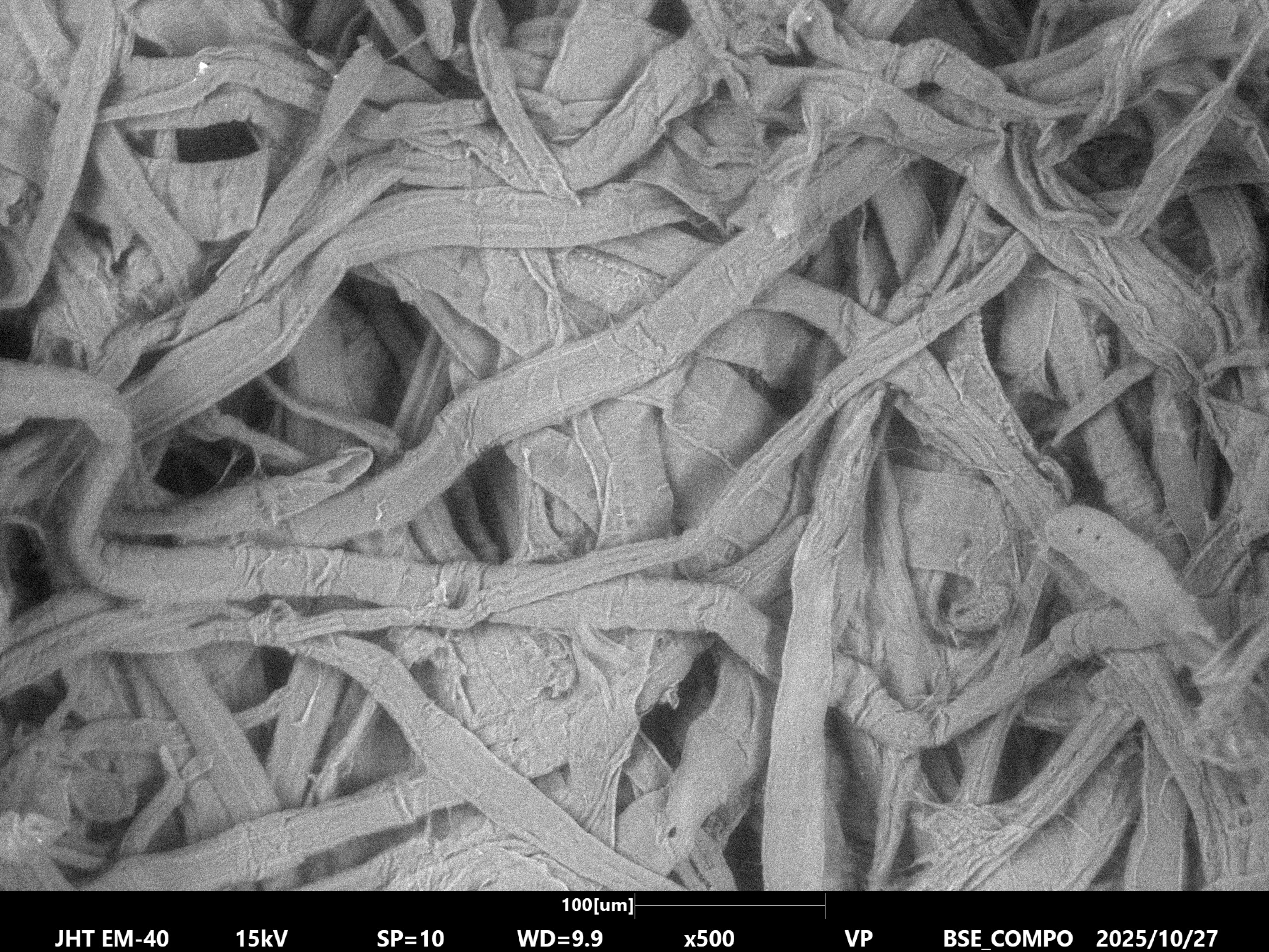
Failure Mechanisms
Every investigation has different requirements. Our applications scientists select the analysis approach based on the question being addressed.
Failure Mechanism | Typical Observations |
Electrostatic Discharge (ESD) | Melted metallization, localized junction damage, burn sites |
Electrical Overstress (EOS) | Extensive metallization damage, thermal degradation, bond pad damage |
Corrosion | Moisture ingress, ionic contamination, oxidation products |
Bond Wire Failure | Lifted bonds, fractured wires, poor intermetallic formation |
Die Cracking | Fracture propagation, stress concentration, package-induced cracking |
Contamination | Foreign material, residues, conductive deposits |
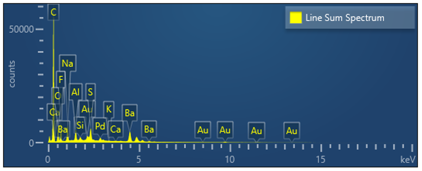
Selecting the Appropriate Technique
Composition at a specific location, useful for identifying particles, inclusions, failure sites, and verifying alloy composition.
Technique | Primary Use | Information Obtained |
Chemical Decapsulation | Die-level evaluation | Direct access to die, bond wires, and bond pads |
Cross Sectioning | Internal package structure | Layer interfaces, solder joints, metallization, voids |
X-ray / CT | Non-destructive inspection | Internal package features without opening the device |
In many investigations, X-ray imaging is performed before decapsulation to document the package condition and identify areas of interest prior to destructive analysis.
Example Applications
ESD Failure Investigation
Objective
Determine the cause of intermittent failures in a communications device.
Results
Decapsulation exposed localized metallization damage adjacent to an input protection structure. Subsequent SEM examination confirmed characteristic features associated with electrostatic discharge.
Conclusion
Failure mechanism consistent with ESD during device handling or assembly.
Counterfeit Semiconductor Investigation
Objective
Evaluate purchased integrated circuits exhibiting inconsistent reliability.
Results
Die markings, die size, and internal construction differed from documented manufacturer specifications.
Conclusion
Evidence supported identification of counterfeit or remarked semiconductor devices
Laboratory Capabilities
Chemical decapsulation is integrated with a range of analytical techniques available within the laboratory, including:
- Optical microscopy
- X-ray and computed tomography
- Cross sectioning
- Scanning Electron Microscopy (SEM)
- Energy Dispersive Spectroscopy (EDS)
- Electrical characterization
- Materials and failure analysis
Combining these methods allows observations made during decapsulation to be correlated with structural, compositional, and electrical data, resulting in a more complete understanding of the failure mechanism.
Important Considerations
Chemical decapsulation is an irreversible process and should be planned as part of an overall analytical strategy. Whenever appropriate, non-destructive inspection methods such as X-ray or CT are performed before package removal to document the original device condition and guide subsequent analysis. Careful process control and thorough documentation help preserve critical evidence throughout the investigation.