Electron Backscatter Diffraction (EBSD)
Microstructural characterization for failure analysis, process validation, and materials reliability assessment.
Technical Summary
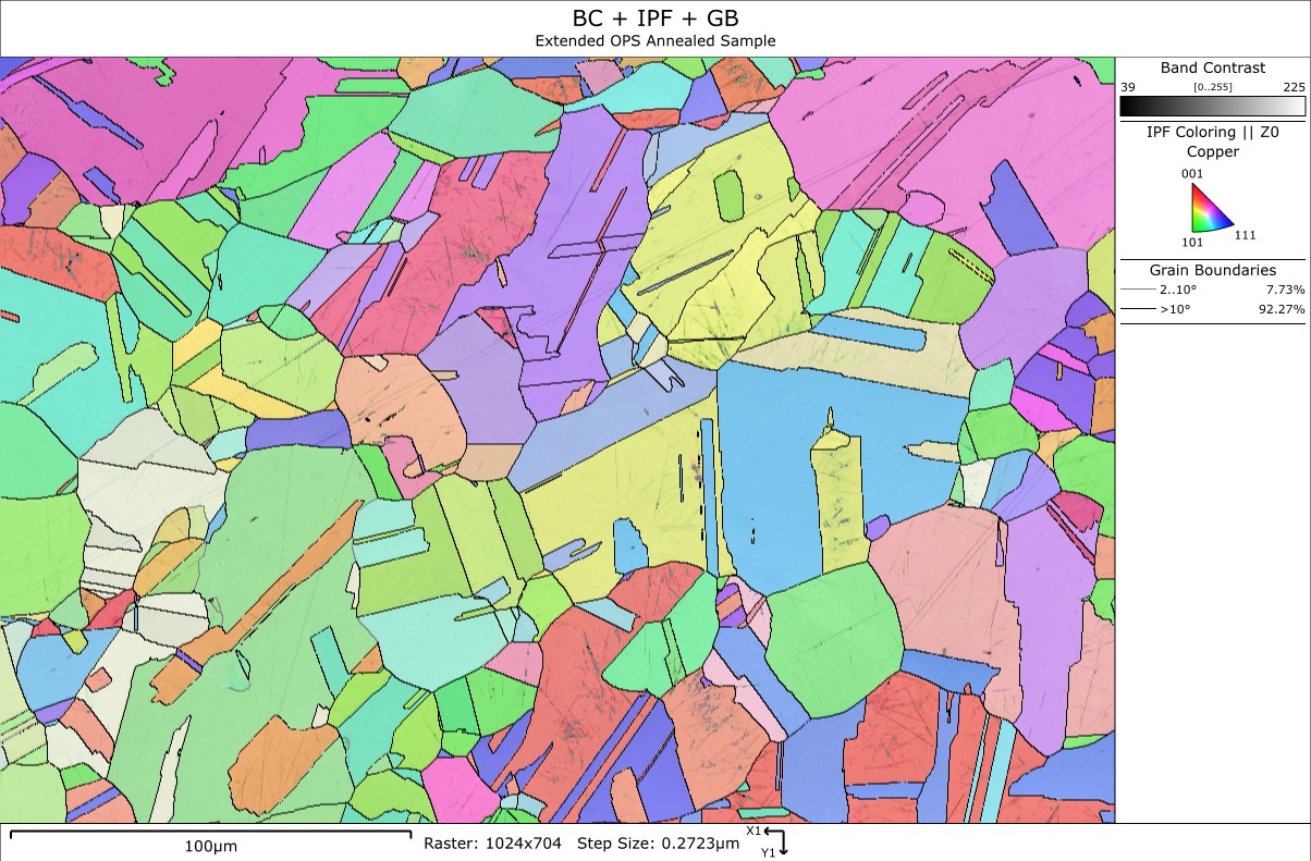
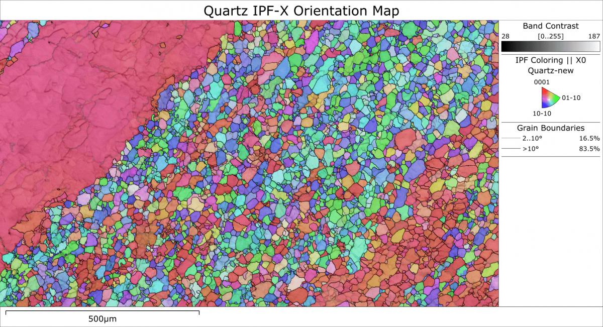
Electron Backscatter Diffraction (EBSD) is an SEM-based technique used to characterize crystalline materials by measuring diffraction patterns generated by backscattered electrons. It provides quantitative information on crystal orientation, grain structure, grain boundary character, crystallographic texture, phase distribution, deformation, and recrystallization behavior.
| Primary output | Quantitative crystallographic orientation and microstructural maps. |
|---|---|
| Typical uses | Failure analysis, heat-treatment validation, process optimization, material qualification, and reliability assessment. |
| Commonly combined with | Scanning Electron Microscopy (SEM), Energy Dispersive Spectroscopy (EDS), and optical microscopy. |
| Sample requirements | Crystalline material, a high-quality prepared surface, and representative sampling. |
Microstructure and Material Performance
Most material failures begin at the microstructural level before damage becomes visible at the surface. Electron Backscatter Diffraction (EBSD) provides a method for measuring crystallographic features that influence material behavior.
Grain size, crystal orientation, phase distribution, deformation history, and recrystallization behavior can influence strength, fatigue life, corrosion resistance, and field performance. When a component fails or a manufacturing process produces inconsistent results, these features can provide evidence of the underlying mechanism.
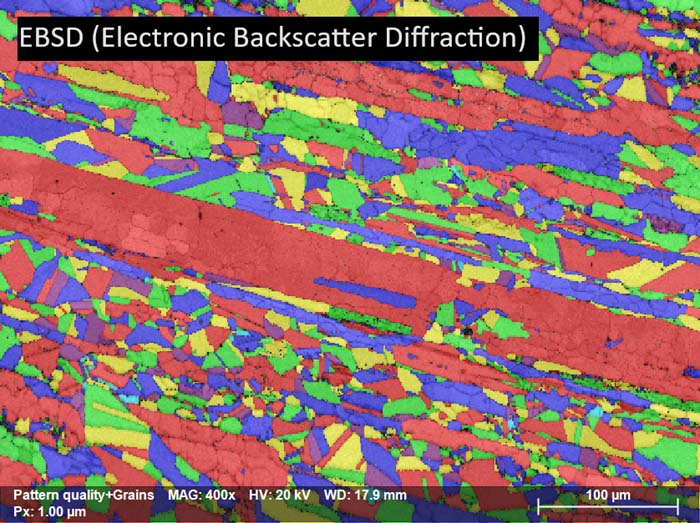
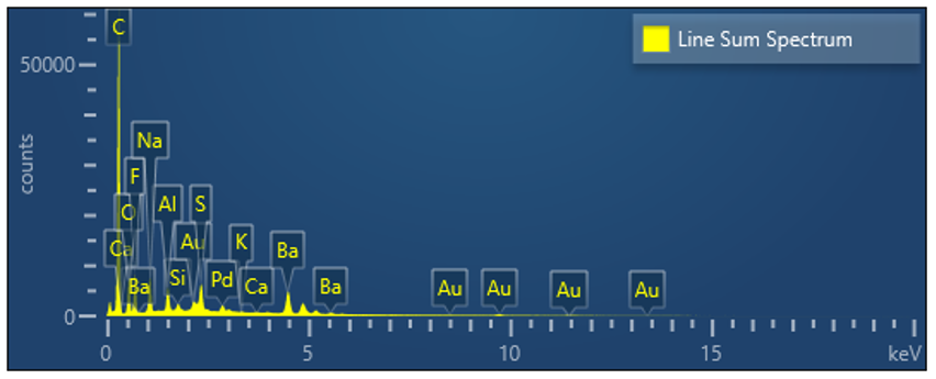
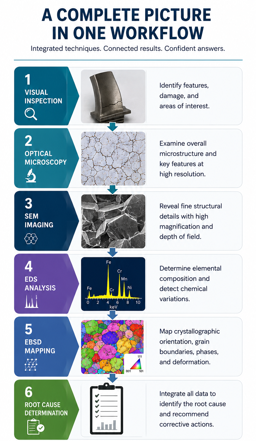
When combined with Scanning Electron Microscopy (SEM) and Energy Dispersive Spectroscopy (EDS), EBSD adds quantitative crystallographic information to structural and compositional analysis.
Why EBSD Is Used
Many material problems are linked to microstructural features that are not fully characterized by optical or conventional SEM imaging alone. Examples include:
- Fatigue cracking
- Stress corrosion cracking
- Weld failures
- Heat treatment inconsistencies
- Grain growth
- Texture-related failures
- Additive manufacturing defects
- Forming and stamping issues
Principle of Operation
Electron Backscatter Diffraction (EBSD) is an SEM-based technique for characterizing crystalline materials.
When an electron beam strikes a tilted crystalline sample, backscattered electrons form diffraction patterns. Analysis of these patterns can provide information on:
- Crystal orientation
- Grain size
- Grain boundary character
- Crystallographic texture
- Phase identification
- Strain and deformation
- Recrystallization behavior
Typical Engineering Questions
- Why did this component fail?
- Has recrystallization occurred?
- Is the heat treatment process producing the intended microstructure?
- What caused the observed grain growth?
- Are weld properties consistent from part to part?
- How is crystallographic texture affecting performance?
- Is additive manufacturing producing the intended microstructure?
EBSD Measurement Capabilities
| EBSD Capability | Engineering Information Provided |
|---|---|
| Grain Size Analysis | Quantitative grain size measurements supporting heat treatment verification, quality control, mechanical property prediction, and process optimization. |
| Grain Boundary Characterization | Identification of high-angle, low-angle, twin, and special grain boundaries that can influence crack propagation, corrosion resistance, and fatigue behavior. |
| Crystallographic Texture | Measurement of preferred grain orientations that can affect strength, formability, and anisotropic behavior in rolled, drawn, stamped, and other processed materials. |
| Phase Identification | Differentiation of phases such as austenite, ferrite, martensite, carbides, and intermetallic compounds when crystallographic distinction is available. |
| Recrystallization Analysis | Mapping of recrystallized, deformed, and recovered regions to support heat treatment validation and process or failure investigations. |
Application Examples
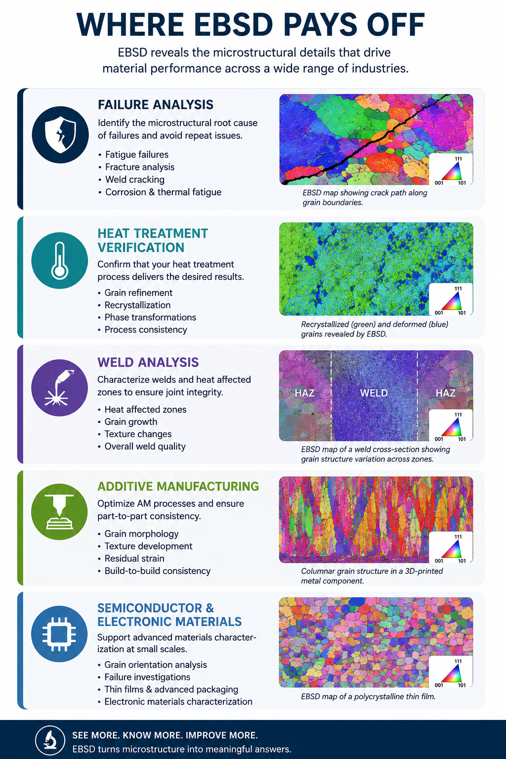
Fatigue Crack Investigation
- Problem
- Repeated fatigue failures in a high-strength alloy component.
- EBSD Result
- Crack propagation followed specific grain orientations, and high-angle grain boundaries accelerated crack growth.
- Interpretation
- Microstructural anisotropy introduced during manufacturing was identified as a contributing root cause and provided a target for redesign.
Heat Treatment Validation
- Problem
- Unexpected hardness variation between production lots.
- EBSD Result
- Incomplete recrystallization and significant grain size variation were observed.
- Interpretation
- An inconsistent heat treatment cycle was identified, allowing the process to be adjusted for improved lot-to-lot consistency.
Additive Manufacturing Qualification
- Problem
- Variability in the mechanical performance of printed components.
- EBSD Result
- Strong texture development and directional grain growth were observed.
- Interpretation
- Laser scan strategy and thermal history were identified as process drivers, informing changes intended to improve part-to-part repeatability.
Integrated Analytical Approach
EBSD results are most useful when interpreted in the context of the material, manufacturing process, and failure mode being investigated. JH Analytical Services combines SEM, EDS, and EBSD to correlate structure, chemistry, and crystallography within a single analytical workflow.
Analytical Scope
- Integrated SEM, EDS, and EBSD
- Root-cause-focused interpretation
- Quantitative data for qualification and design decisions
Application Areas
- Aerospace and automotive
- Energy and medical
- Additive manufacturing
- Electronics
Sample Preparation Requirements
Successful EBSD analysis depends strongly on surface condition. Damage-free, well-prepared surfaces are required to produce high-quality diffraction patterns and reliable orientation data.
Preparation Methods
- Precision sectioning
- Mechanical polishing
- Final colloidal silica polishing
- Ion milling for challenging materials
Core Requirements
- Crystalline material
- High-quality surface preparation
- Representative sampling
Analytical Considerations
EBSD should be planned as part of an overall analytical strategy. The technique requires crystalline materials, high-quality surfaces, and representative sampling. When appropriate, EBSD can be combined with SEM imaging, EDS analysis, optical microscopy, and other analytical methods to provide a more complete understanding of material behavior and failure mechanisms.
Technical Questions and Answers
Concise answers to common engineering questions about EBSD, stated in a form suitable for technical reference and retrieval.
What is Electron Backscatter Diffraction (EBSD)?
EBSD is an SEM-based technique for characterizing crystalline materials. Diffraction patterns generated by backscattered electrons are analyzed to measure crystallographic orientation and related microstructural features.
What can EBSD measure?
EBSD can provide information on crystal orientation, grain size, grain boundary character, crystallographic texture, phase identification, strain and deformation, and recrystallization behavior.
How is EBSD used in failure analysis?
EBSD can relate crack paths, grain orientation, grain boundary character, texture, phase distribution, and deformation features to a failure mechanism, supporting root-cause investigation.
What sample conditions are required for EBSD?
EBSD requires crystalline material, high-quality surface preparation, and representative sampling. Surface condition directly affects diffraction-pattern quality and the reliability of orientation data.
Why combine EBSD with SEM and EDS?
Combining EBSD with SEM imaging and EDS analysis allows crystallographic information to be interpreted alongside structural and compositional information, providing a more complete view of material behavior.
Conclusion
EBSD provides a quantitative link between microstructure and material performance. By measuring grain structure, crystallographic texture, phase distribution, and deformation behavior, the technique can support investigations involving manufacturing, reliability, qualification, and failure analysis.
Combined with SEM imaging and EDS elemental analysis, EBSD can provide a more complete view of material behavior and improve the technical basis for process-control, quality, and design decisions.