Note: Within this paper, “MEMS device” refers only to the subset of semiconductor MEMS devices.
The Mighty MEMS
Envision a microphone. You probably conjure a spherical or oblong metallic mesh with a band about its equator sitting atop a black and slightly tapered cylindrical handle. If you’re familiar with the entertainment industry, maybe you also picture a circular pop filter on a gooseneck mount for a more professional setup.
What most people don’t imagine, however, is a 1.5mm square silicon chip with a ~5-10µm thick and 1mm wide diaphragm. And yet, despite our preconceived notions, handheld and professional models comprise less than 1% of microphone sales, with the modest semiconductor MEMS device accounting for nearly the entire remainder at well over a billion units sold annually.
What is a MEMS Device?
MEMS is an acronym for Micro-Electro-Mechanical Systems. It refers to a class of devices that combine both moving mechanical and electrical parts.
In short, moving parts affect electrical signals through the die, or voltage biases can be used to direct moving parts. Commonly used MEMS devices include accelerometers, gyroscopes, pressure sensors, magnetic field sensors, and steerable mirrors.
In consumer products, MEMS devices are widespread. Applications include digital compasses, airbag deployment sensors, inkjet printer heads, blood pressure sensors, LiDAR mirrors, and, of course, microphones.
MEMS Device Fabrication: The Secret to Success
One key accelerant in the explosive development and mass adoption of MEMS devices is the relative ease of fabrication. Furthermore, manufacturers take advantage of advanced epitaxy, deposition, etching, and lithography processes developed by the semiconductor industry by building these devices out of common semiconductors like silicon. As a result of their small footprints and increasing durability, MEMS devices have become increasingly integral to the most popular electronic device on the planet: phones.
Microphone MEMS Device Construction and Function
Sounds are simply a series of pressure waves in the air within a specific frequency range. Much like a speaker vibrates to create these waves, the MEMS microphone has a several-micron-thick diaphragm that vibrates in response to sound waves.
In addition and adjacent to this diaphragm is the backplate, a rigid porous structure coated with a conductive film. By actively measuring the capacitance between the diaphragm and backplate, the small vibrations induced in the diaphragm by sound waves translate into an electrical signal.
Deconstructing a Smartphone MEMS Microphone
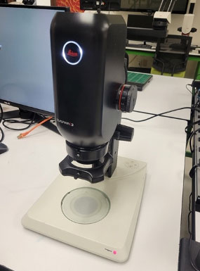
For sound waves to reach the diaphragm, there must be a path from the outside world to the diaphragm. In order to examine this, we deconstructed the phone, extracted two microphones, and analyzed and documented them using a Leica Emspira 3 digital microscope.
You might ask yourself: why does a phone need more than one microphone? In short, your phone needs to hear you speak; in addition, it must “listen” to your surroundings to apply noise cancellation, monitor audio, and mitigate feedback during your speakerphone calls.

Preparing and Examining the Microphone’s Mesh Screen
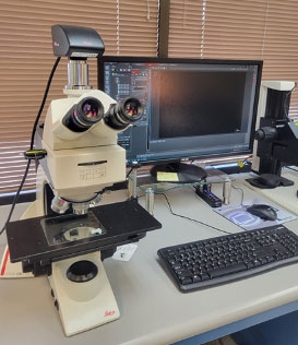
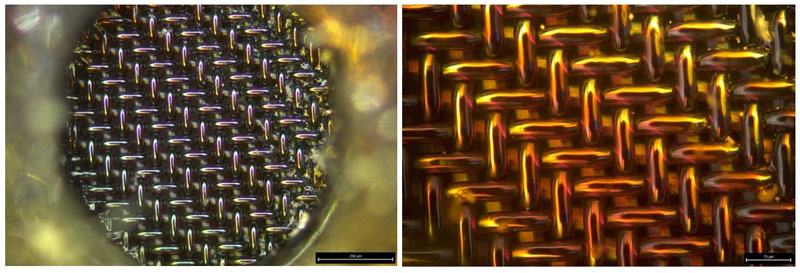
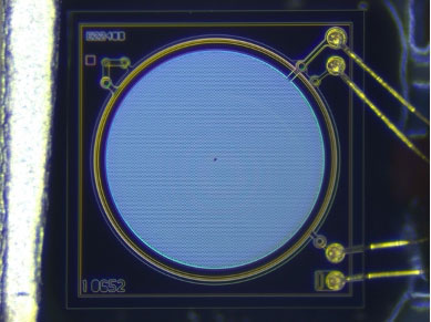
MEMS device #1 has a fine mesh screen covering the hole leading to the diaphragm. This mesh serves as a protective barrier to prevent particulates and water from reaching the microphone. Also, the mesh is tightly woven and constructed of material that water does not penetrate. The result is a series of holes through which air can pass but water will not. We imaged the mesh using a Leica DM2700 compound microscope with a Leica K5C digital camera.
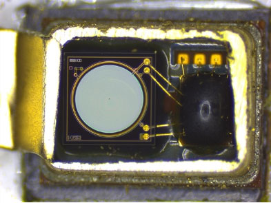
Due to their extremely thin diaphragm and backplate, de-lidding microphones is challenging, and preventing particle introduction is critical. A failed microphone may contain particles or contamination on the diaphragm, which is challenging to diagnose. In addition, cleaning these delicate structures puts them at significant risk of damage. Therefore, once particles have settled on the surface of a microphone, they are often left.
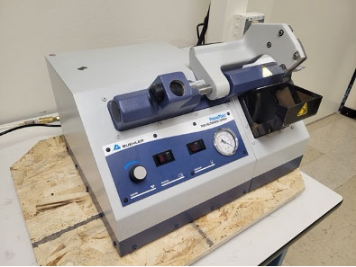
We thinned the package lid using a Buehler PetroThin Sectioning System. Then, we mechanically cut and lifted the lid using techniques developed to minimize particles.
Scanning the Semiconductor Die
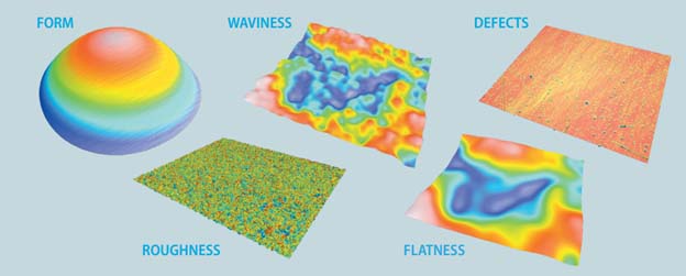
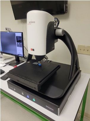
We scanned the die surface using a Sensofar S neox in both confocal and interferometry modes and found the latter better suited for this sample. Next, we reconstructed the data into a 3D model using SensoView software.
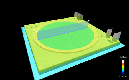
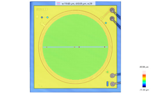

After aligning the model to a flat plane, we drew a line profile across the backplate to measure planarity along this axis. Incredibly, we found only 10s of nanometers of deflection.

Next, we drew another line profile to measure the standoff height between the backplate and the diaphragm. We measured a consistent 2.18µm near the center of the die.

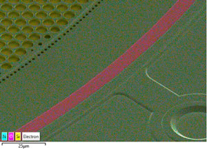
After collecting interferometry data, we coated the sample in AuPd (gold-palladium) and collected scanning electron microscope (SEM) images of the various structures using a ThermoFisher Apreo S field emission SEM.


A brief Energy Dispersive X-ray Spectroscopy (EDS) map confirmed the presence of silicon nitride, silicon dioxide, and silicon as the primary constituents of this MEMS microphone. The utilization of these materials contributed significantly to the accelerated development of microphones and other MEMS devices.
The Impact of MEMS Devices
From the early hardwired and range-limited telephone to the modern supercomputer that we call the smartphone, microphones facilitate communication over long distances. The fact that we can construct such a MEMS device out of a ~1.3×1.3mm die is incredible.
The MEMS market continues to grow as novel manufacturing techniques decrease costs and footprints while improving performance. In fact, your smartphone includes upwards of a dozen MEMS devices working tirelessly to provide you with an optimal user experience. The phone has evolved at a blistering pace to become the world’s most popular electronic consumer product. While we can assume that Alexander Graham Bell’s future vision didn’t include millimeter-scale gyroscopes embedded in our phones, we are sure he would be impressed.
Need help with Sample Imaging for your application?
Complete the form on this page or contact us.

