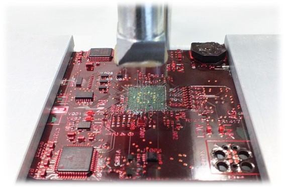
PCB and Electronics

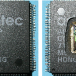
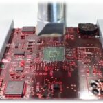
In our lab we see a wide array of applications involving microelectronic and micro-mechanical parts, and assembly of those parts.

This class of applications stretches across a wide swath of industries from defense and consumer electronics to telecommunications and photonics. Today you are hard pressed to find a device that doesn’t have some microelectronic or micro-mechanical parts in it. Printed Circuit Boards or PCBs are everywhere.

We help you see your PCB and electronics products clearly at every phase of the production process:

  • Design verification
  • Assembly
  • Quality assurance and inspection
  • Defect analysis

Related Content

Contact Us

Recent Posts

Unlocking Material Performance with EBSD

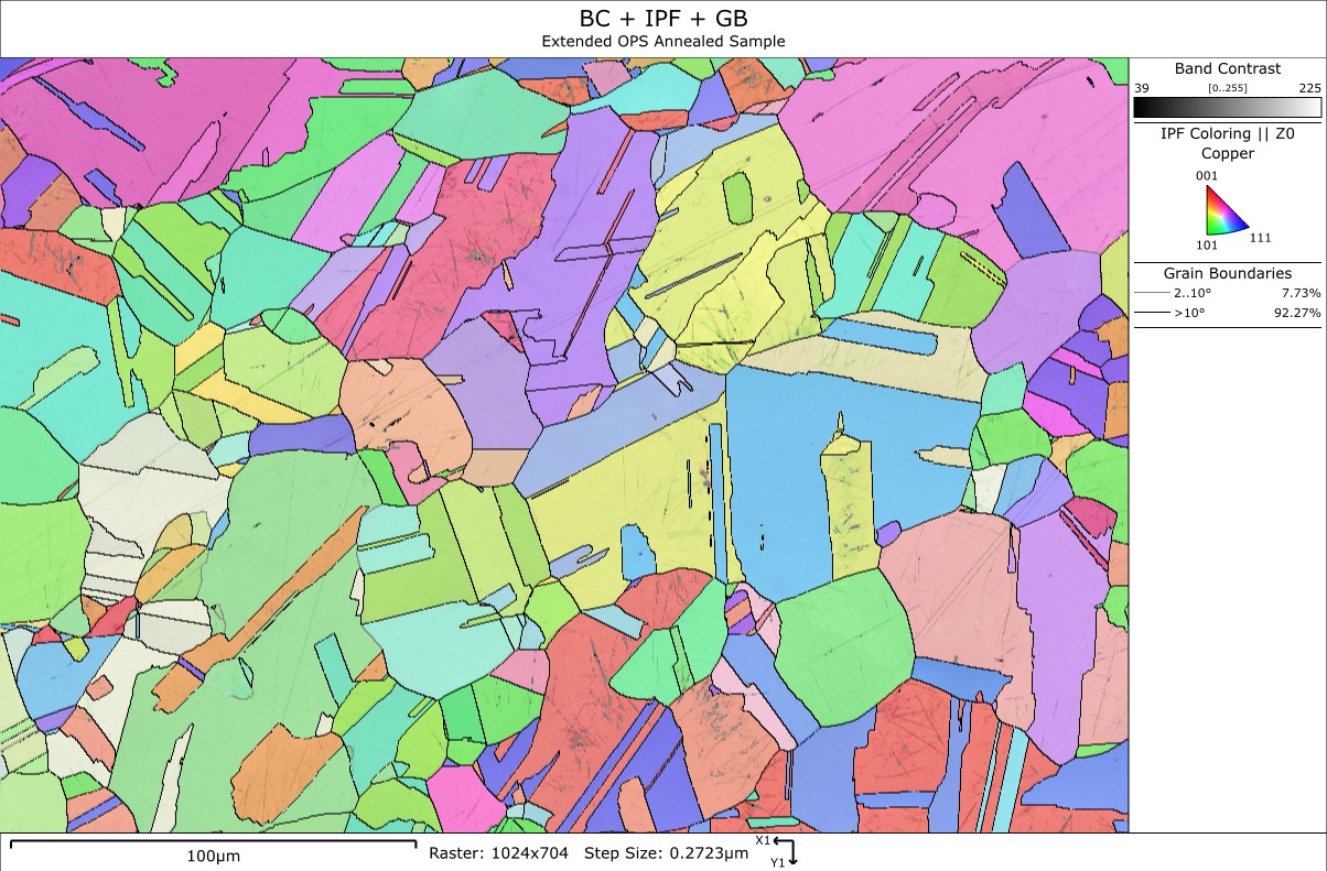
Materials Characterization / Technical Article Electron Backscatter Diffraction (EBSD) Microstructural characterization for failure analysis, process validation, and materials reliability assessment. Author: Tim SchoenRole: Lab Director, JH Technologies Technical contents Summary

Read More »

Chemical Decapsulation

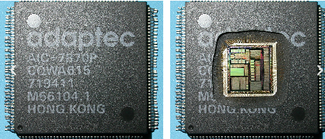
Author Tim Schoen, Lab Director, JH Technologies Access the Die. Preserve the Evidence.   Chemical decapsulation is a controlled sample preparation technique used to remove the plastic encapsulant from semiconductor

Read More »
EDS-chart-with-elements

Elemental Analysis: SEM+EDS

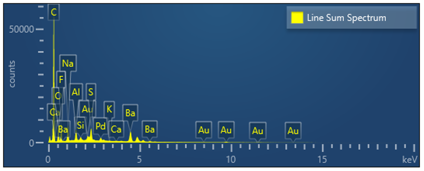
Author Tim Schoen, Lab Director, JH Technologies Understand What Your Material Is Made Of When a contaminant, corrosion site, or unknown particle appears, EDS analysis from JH Technologies helps identify

Read More »

CONTACT US