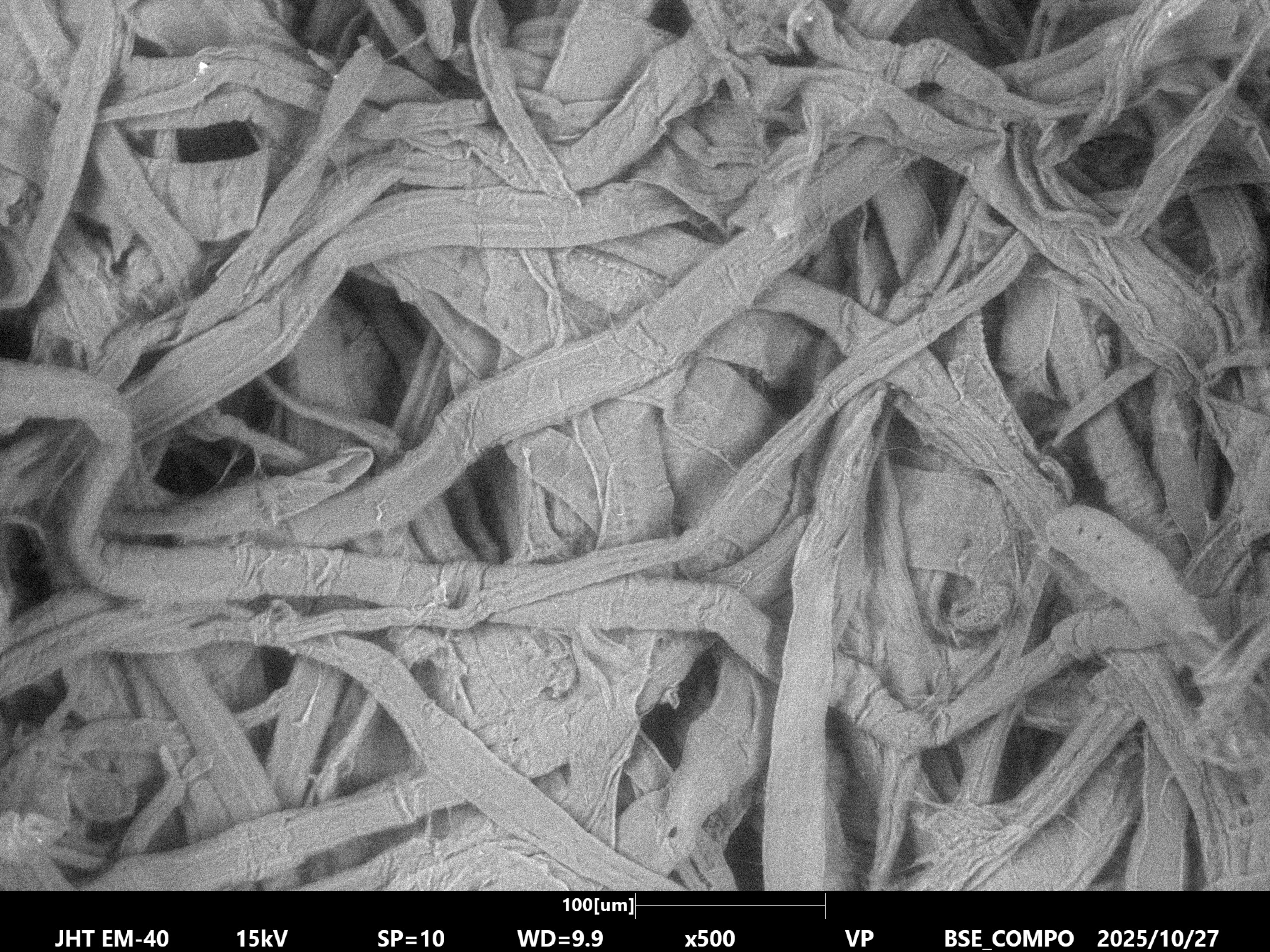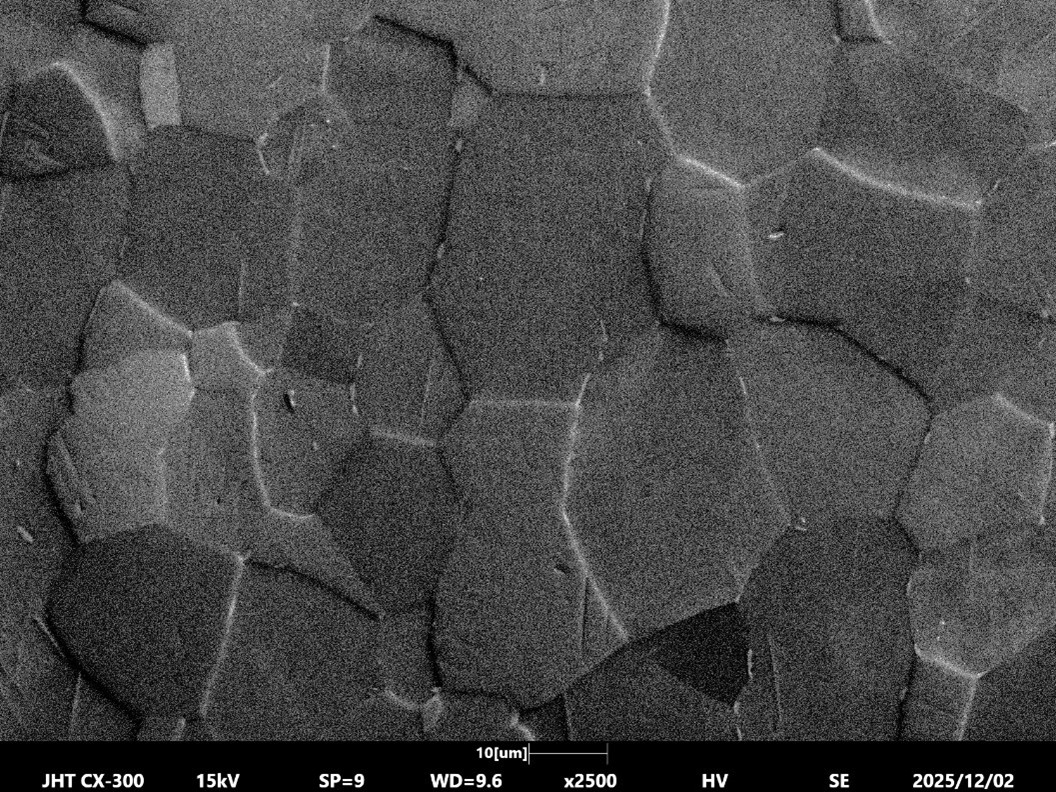
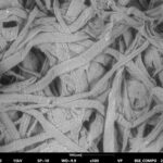
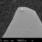
Scanning Electron Microscopy (SEM) is a powerful imaging technique used to inspect the surfaces of solid samples at high magnification. Some SEM systems are capable of sub-nanometer resolution at magnifications up to 1,000,000x. As a result, they can produce images showing sample surface morphology, composition, and microstructure. While there are many unique configurations, all SEMs utilize a focused beam of electrons to scan a sample’s surface and generate images based on the interactions between the electrons and the sample.
SEM Applications
Scanning electron microscopy is used extensively in various applications, including:
- Material Analysis: SEM allows researchers to study microstructure, surface morphology, and composition. It is particularly valuable for identifying contaminants, defects, or structural changes in materials. EDS and EBSD, two techniques indispensable for material analyses, are outlined further down this page.
- Failure Analysis: Manufacturers and consumers frequently utilize SEM to investigate the root cause of component failures. SEMs can provide insights into the failure mechanisms, such as fatigue, corrosion, micro-cracks, sub-micron electrical damages, or manufacturing defects.
- Quality Control: SEMs ensure the quality and consistency of products. They allow for detailed inspections of surface features, dimensions, and uniformity, helping to identify deviations or anomalies.
- Nanotechnology Research: SEM is indispensable for studying nanomaterials and nanoscale structures. It enables researchers to characterize nanoparticles, nanostructures, and thin films, contributing to advancements in fields like electronics, batteries, and medicine.
Scanning Electron Microscopy–Additional Capabilities
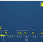
SEMs can be equipped with hardware to enable chemical analysis, crystallographic analysis, and more. The most common SEM attachment is known as an Energy Dispersive X-Ray Spectroscopy (EDS or EDX) detector. These detectors capture and measure characteristic X-ray emissions from samples during electron beam scanning. Individual elements have unique characteristic X-ray emissions, and by measuring the X-ray photon energy, operators can map and quantify the elemental composition of a sample.
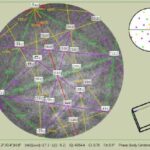
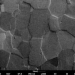
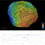
Less common attachments for SEMs include Wavelength Dispersive X-Ray Spectroscopy (WDS) detectors and Electron Backscatter Diffraction (EBSD) detectors. While WDS serves a function similar to that of EDS, EBSD is unique. In short, as the SEM scans a crystalline sample (e.g., metal grains) with the electron beam, the electrons diffract in a specific pattern and form a pattern that is captured on a fluorescent screen. From those patterns, an operator can map out grain boundaries, lattice structures, crystal orientations, dislocations, and more.
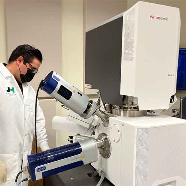
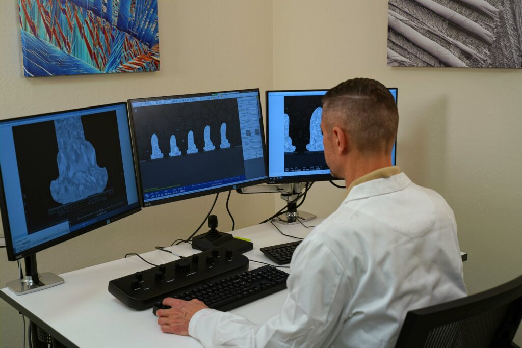
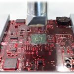
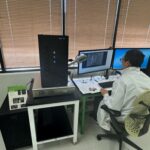
Scanning Electron Microscopy Services at JH Analytical
JH Analytical Labs provides complete SEM, EDS, and EBSD services.
Below is our equipment lineup in the lab:
- ThermoFisher Scientific Apreo S field emission scanning electron microscope equipped with:
- EDS: Oxford Ultim Max 100 silicon drift detector (SDD), with a 100mm2 window
- EBSD: Oxford Symmetry S2 electron backscatter diffraction detector
- Coxem EM-30AX tabletop scanning electron microscope equipped with:
- EDS #1: Oxford Xplore compact detector with a 30mm2 window
- EDS #2: Bruker Nano XFlash 6-30 detector, with a 30mm2 window
- EBSD: Bruker e-Flash XS electron backscatter diffraction detector
SEM Imaging and Analysis – Related Articles
- Elemental Analysis: SEM+EDS
- Dye & Pull Analysis: Revealing Hidden Failure Mechanisms in Electronic Assemblies
- Low Vacuum SEM: Faster Results with Less Sample Preparation
- How To: Prepare Titanium for Optimal EBSD Analysis
- 430 Year Old Coin Under The Microscope
- Are Candy Wrappers Safe for Your Kids?
- Solder Joint Failure: WHITE PAPER

- What is in a Lug Nut or Any Other Sample? [Application Note]
- Memory Device Cross-Sectioning [Learn from the JHA Team]
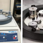
- 4 Benefits of Vibratory Polishing
- What is the best method to prepare a sample for EBSD? [Application Note]