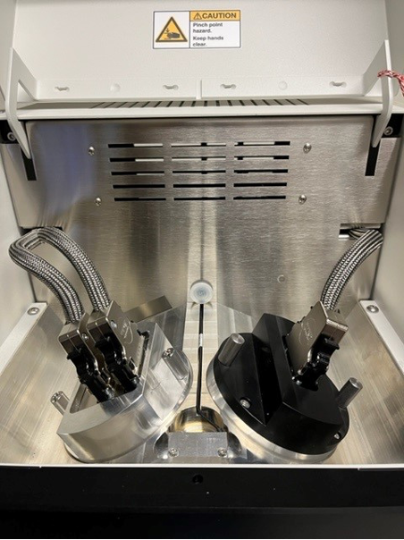
Non-conductive samples absorb and accumulate electrons (charging) when processed with conventional high vacuum, high voltage scanning electron microscopes (SEMs). As a result, images glow or turn black, and the SEM generates poor imaging. Sputter coating solves this issue.
Sputter coating is a deposition process that grounds your specimen by covering it with a thin, conductive material layer—typically metal—to improve imaging significantly.
You can use low vacuum and environmental SEMs with non-conductive samples, but they are limited in magnification and resolution.
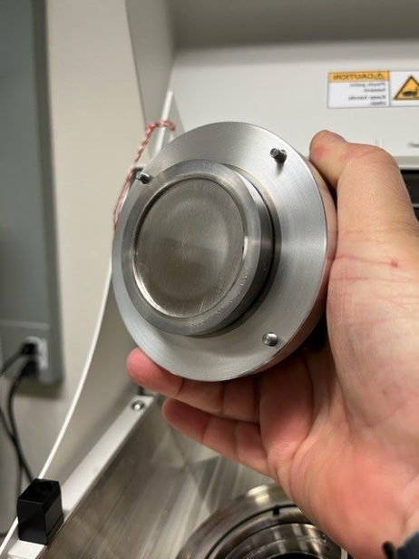
Choosing a Sputter Coater
The most common sample coatings are gold (Au), blends of gold palladium, and other noble metals, particularly from the platinum group of elements, which do not easily oxidize. When choosing a metal, consider what materials are in the sample and what size of metal particle you want.
For example, if you are imaging a gold sample, you do not want to coat it with gold, especially if you want to perform elemental analysis.
Benefits of Metal Coatings
Metal coatings prevent sample charging, increase the signal-to-noise ratio (heavy metals are good secondary electron emitters) when imaging, and create better images of surface topography.
If you need to remove a coating from a sample post-imaging without physical sample preparation, silver (Ag) is the best metal to use. Using a mild-nitric acid solution, you can strip the surface of a silver (Ag) coating without damaging the sample. Then, the sample can be used and processed again without worry of coating contamination.
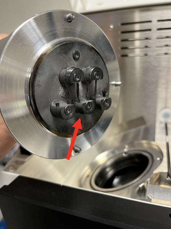
Carbon Sputter Coating
A carbon coating can also be sputtered or evaporated to provide a conductive layer when a metal is not the optimal choice. It is an excellent choice for x-ray spectroscopy and elemental analysis as it prevents mixing information from the coating and the sample. EBSD (electron backscatter diffraction) also uses carbon coatings, where the main goal of the investigation is to understand the surface and grain structure. If the coating were metallic, the grain structure information would be affected, ultimately changing the data and resulting in improper analysis.
Sputter Coaters
Every SEM lab needs a sputter coater, assuming some samples are not conductive.
Basic Sputter Coaters
When you work with lower magnification SEMs, basic sputter coaters work well and can be inexpensive and easy to use and maintain. These coaters operate with low vacuum and atmospheric air to deposit 10-20nm coatings, which at lower SEM magnifications, will not affect imaging.
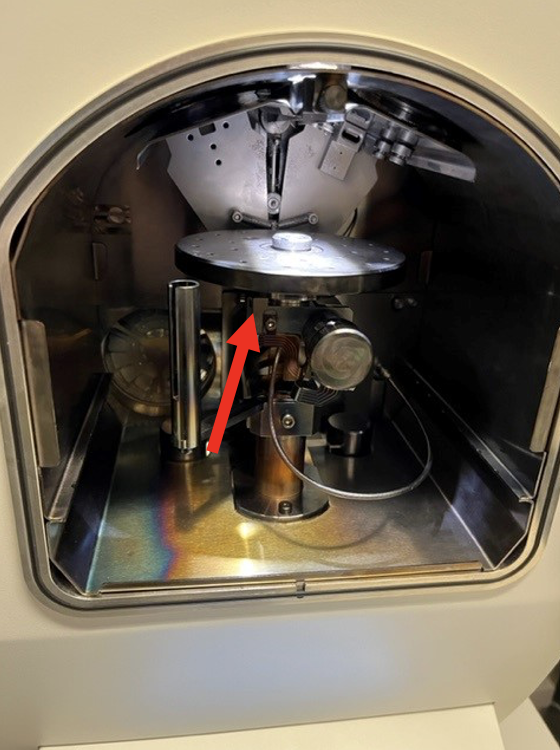
High-End Sputter Coaters
For higher magnifications, especially with SEMs that have <5nm resolution, coating thicknesses of 10nm-20nm will be evident in your images and obscure sample details smaller than the coating thickness.
High-end sputter coaters offer high vacuum, inert gas to improve the plasma generated, and film thickness monitors essential to precision coating, enabling you to deposit coatings as thin as 1nm. Thinner coatings are also vital for EBSD analysis. A rotating and tilting stage helps you achieve thin, even coatings, especially in samples with large surface topography, such as rocks, insects, and MEMs devices.
JH Analytical Labs Sputter Coaters
Our lab uses both types of coaters:
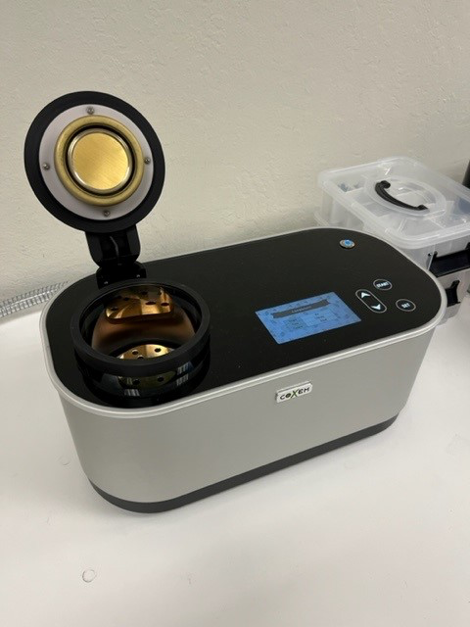
- The COXEM SPT-20, a basic coater for everyday work with lower magnification and low vacuum
- The Leica ACE600, an Argon gas coater for tighter coating control needs, allowing us to rotate and tilt samples for a more even coating, set the exact coating thickness, and choose between a carbon or metal coating
Below is the COXEM SPT-20 sputter coater with a gold target used for standard imaging.
Related Article: Proper Maintenance and Cleaning of Your Sputter Coater
Need help with your lab application?
Complete the form on this page or contact us.

