Author Tim Schoen, Lab Director, JH Technologies
Controlled Surface Preparation for Microstructural Analysis
Sharper Patterns. Faster Maps. Deeper Insight.
A polished sample can look smooth under an optical microscope and still contain enough surface damage to compromise electron microscopy. Fine scratches, smeared phases, embedded abrasive, residual strain, oxide, and contamination may all alter what an SEM, EDS detector, or EBSD camera records.
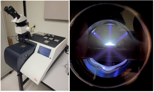
— Leica EM TIC 3X Ion Mill using 3 ion guns
What is ion flat milling?
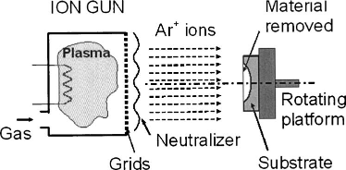
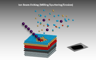
Ion flat milling is a broad-beam sample-preparation technique. Inside a vacuum chamber, argon gas is ionized and the resulting Ar+ ions are accelerated toward the specimen. When the ions strike the surface, momentum transfer ejects surface atoms in a process called physical sputtering.
The beam approaches the surface at a shallow angle while the sample rotates or rocks. This motion distributes the ion dose across a wider area and reduces directional artifacts. The goal is not to cut deeply into the specimen. It is to remove the mechanically affected surface layer and improve the area that will be examined.
Argon is commonly used because it is inert and sufficiently massive for sputtering. That does not make the process completely damage-free. Excessive beam energy, current, time, or heat can produce new artifacts, including preferential sputtering, redeposition, pitting, or ion-induced disorder.
Why the prepared surface matters
SEM, EDS, and EBSD interrogate the near-surface region of a specimen. A prepared surface is therefore part of the measurement system, not merely a cosmetic finish. The preparation method can expose the material faithfully or create a modified layer that is later interpreted as microstructure.
Surface artifact | Common source | Possible analytical effect |
Residual deformation | Grinding or aggressive polishing | Weak EBSD patterns and altered channeling contrast |
Smearing | Ductile phases or soft and hard interfaces | Hidden pores cracks or displaced phase boundaries |
Relief | Different polishing rates among phases | Focus variation and geometry dependent EDS response |
Embedded abrasive | Grinding and polishing media | Foreign particle contrast or misleading elemental peaks |
Oxide or contamination | Air water chemistry or handling | Changed surface chemistry and unstable signals |
Where ion milling adds value
Mechanical grinding and polishing remain efficient ways to create a flat specimen and remove bulk material. Ion milling is usually most effective as the final preparation step rather than a replacement for the complete mechanical sequence.
It is especially useful for:
- Metals and alloys prepared for EBSD mapping or electron channeling contrast
- Multiphase materials that develop relief during polishing
- Coatings and thin films with interfaces that can smear or round
- Semiconductor structures and electronic assemblies
- Ceramics composites battery materials and selected polymers
- Samples that should not be exposed to aqueous polishing media
How flat milling differs from other ion milling methods
Flat milling treats an existing surface over a comparatively broad area. Cross-section milling uses a mask to define an edge and expose internal layers below that edge. Focused ion beam milling works on a much smaller, precisely selected region and is valuable for site-specific sectioning. These approaches solve different preparation problems and should not be treated as interchangeable.
The variables that control the result
There is no universal ion-milling recipe. Sputter yield and surface response depend on the specimen as well as the instrument settings. The most important variables are:
- Beam energy. Higher energy generally increases material removal but may increase damage depth and heat. A lower-energy final step can reduce the altered layer.
- Ion current. Current controls dose rate and contributes to thermal load.
- Incidence angle. Angle changes sputter yield and the way topography develops across different phases.
- Milling time. Time controls total ion dose, but removal depth should be calibrated rather than assumed.
- Sample rotation or rocking. Motion averages the beam direction and helps limit striations and uneven treatment.
- Cooling or intermittent milling may be needed for polymers, solder, adhesives, battery materials, and other heat-sensitive specimens.
A scientifically useful method records all of these variables along with vacuum conditions, sample orientation, cleaning, and transfer time. Changing one factor at a time makes optimization easier to interpret.
Example reduction in polishing topography
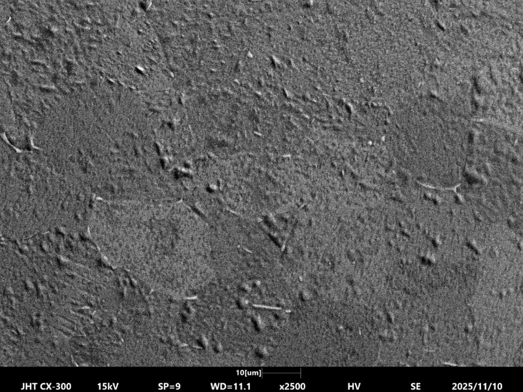
In a JH Technologies preparation trial, a specimen was mechanically polished with Buehler 0.05 micrometer MasterMet suspension and then flat milled on a COXEM system at 4 kV for one hour. The comparison images show less fine polishing texture after ion milling.
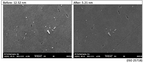
SEM images before and after flat milling. The original test record reported roughness values of 12.52 nm and 5.21 nm respectively.
The reported value decreased by approximately 58 percent. That result is encouraging, but it should be interpreted as a result for this specimen and this preparation recipe, not as a universal performance claim. Milling response changes with composition, phase distribution, crystallographic orientation, topography, beam settings, and the way roughness is measured.
For a reproducible ISO 25178 comparison, the record should identify the specific areal parameter, such as Sa or Sq, as well as the scan area, lateral sampling, filtering, measurement instrument, and number of replicate locations. A number labeled only as roughness is not sufficient for quantitative comparison.
How to verify that the surface is ready
A surface that appears smoother is not automatically ready for analysis. The acceptance test should match the analytical objective.
- For SEM, compare scratch density, edge definition, charging behavior, and repeatable secondary-electron or backscattered-electron contrast.
- For EDS, check spectral stability, contamination peaks, and consistency across phase boundaries under fixed acquisition conditions.
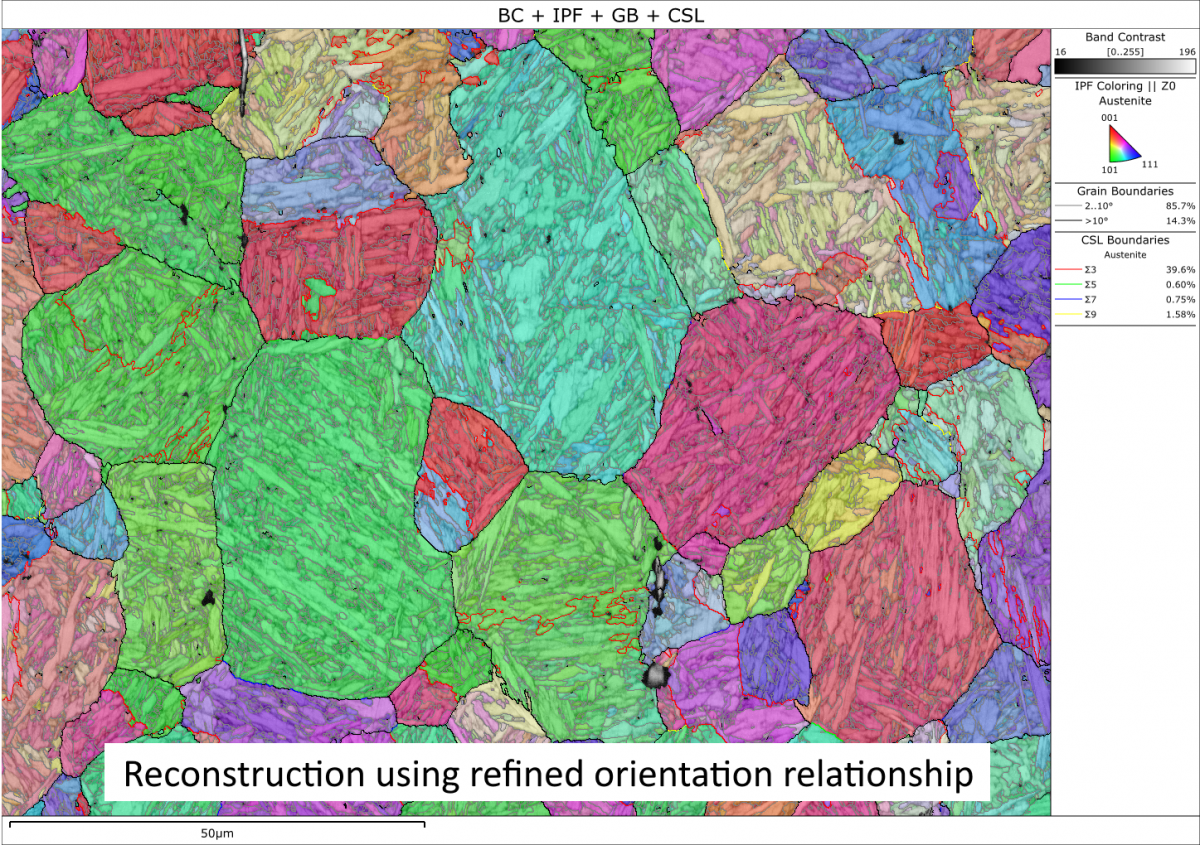
- For EBSD, compare indexing rate, pattern quality, mean angular deviation, and the spatial distribution of non-indexed points.
- For surface metrology, report a named ISO 25178 parameter together with the scan size and filter settings.
A practical flat milling workflow
1) Define the analytical question Identify the feature size, required area, and whether the endpoint is morphology, composition, crystallography, or roughness.
2) Prepare the geometry Section, mount, grind, and polish until the specimen is planar and free of deep scratches.
3) Clean and load Remove loose residue, use clean holders, and minimize uncontrolled handling or air exposure.
4) Start conservatively Select moderate beam conditions and use timed increments during method development.
5) Finish at lower energy when needed Reduce energy or current for the final interval when near-surface damage is a concern.
6) Verify with the intended technique Evaluate the surface using SEM, EDS, EBSD, or metrology rather than appearance alone.
7) Document the recipe Record the full preparation sequence and acceptance metric so the result can be repeated.
Frequently asked questions about ion flat milling
Does ion flat milling replace mechanical polishing?
Usually not. Mechanical preparation creates the geometry and removes bulk material. Flat milling is commonly used afterward to reduce the remaining damaged layer and surface residue.
Why can flat milling improve EBSD?
EBSD is sensitive to residual strain and amorphous surface damage. Removing the mechanically deformed layer can improve Kikuchi-pattern quality and indexing reliability if the ion beam is properly controlled.
Can ion milling change EDS results?
Yes. It can remove contamination, but preferential sputtering or redeposition may alter near-surface composition. Critical measurements should be checked against controls.
How much material does ion flat milling remove?
The amount depends on material, beam energy, current, incidence angle, time, and specimen motion. The removal rate should be calibrated on a representative sample.
Can ion milling damage the specimen?
Yes, if the dose or thermal load is excessive. Possible effects include heating, pitting, redeposition, preferential sputtering, implantation, and near-surface disorder.
The central takeaway
Ion flat milling can improve the reliability of SEM imaging, EDS microanalysis, and EBSD mapping by removing a thin layer affected by mechanical preparation. Its value comes from control, not simply from ion exposure. A defensible workflow uses material-specific conditions, limits heat and beam damage, and verifies the result with a metric tied to the intended analysis.
Suggested web metadata
Page title: Ion Flat Milling for SEM EDS and EBSD Sample Preparation
Meta description: Learn how broad-beam argon ion flat milling reduces polishing damage and prepares metals, coatings, semiconductors, ceramics, and composites for SEM, EDS, and EBSD analysis.
Suggested URL: /ion-flat-milling-sem-eds-ebsd-sample-preparation/
Technical references
Leica Microsystems. High Quality EBSD Sample Preparation. Technical article
Erdman N Campbell R and Asahina S. Precise SEM Cross Section Polishing via Argon Beam Milling. Microscopy Today. JEOL application reprint
Hitachi High-Tech Europe. Sample Preparation and Cleaning Systems. Broad argon ion milling overview
ISO 25178 series. Geometrical Product Specifications Surface Texture Areal.