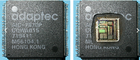
The Semiconductor application space includes both front-end of line (FEOL) and back end of line (BEOL) semiconductor production and R&D processes.
Much of the production and R&D processes take place while the semiconductor products are still in wafer form. Thus, microscopes capable of handling and inspecting wafers with continuously decreasing feature sizes are essential.
JH Analytical Labs is equipped with the right tools and expertise to process and analyze semiconductor devices at every level of production.
Contact us today for assistance with your semiconductor applications.