Semiconductor

The Semiconductor application space includes both front-end of line (FEOL) and back end of line (BEOL) semiconductor production and R&D processes.

Much of the production and R&D processes take place while the semiconductor products are still in wafer form. Thus, microscopes capable of handling and inspecting wafers with continuously decreasing feature sizes are essential.

JH Analytical Labs is equipped with the right tools and expertise to process and analyze semiconductor devices at every level of production.

Contact us today for assistance with your semiconductor applications.
Related Content

Contact Us

Recent Posts

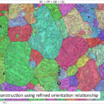
Unlocking Material Performance with EBSD

Materials Characterization / Technical Article Electron Backscatter Diffraction (EBSD) Microstructural characterization for failure analysis, process validation, and materials reliability assessment. Author: Tim SchoenRole: Lab Director, JH Technologies Technical contents Summary

Read More »

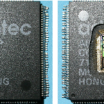
Chemical Decapsulation

Author Tim Schoen, Lab Director, JH Technologies Access the Die. Preserve the Evidence.   Chemical decapsulation is a controlled sample preparation technique used to remove the plastic encapsulant from semiconductor

Read More »
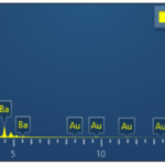
EDS-chart-with-elements

Elemental Analysis: SEM+EDS

Author Tim Schoen, Lab Director, JH Technologies Understand What Your Material Is Made Of When a contaminant, corrosion site, or unknown particle appears, EDS analysis from JH Technologies helps identify

Read More »

CONTACT US