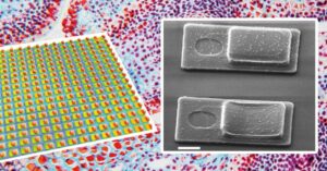
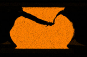
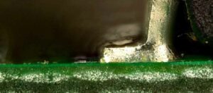
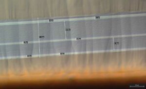
Mapping Capabilities – Apreo SEM
We have incorporated mapping capability for our Apreo SEM Combining and overlaying EDS Element maps on an electron image to make one informative colored image is fast becoming a common
This case study explains measuring membrane deflection for biological sensors in a non-destructive way using an optical profiler vs. SEM.
SERIES Part 1: The Journey of an Electronic Device Through the Analytical Lab In the first article of this series, you will experience the steps of a typical workflow used
Producing Memory Device Cross-Sectioning Samples Our newest JH Analytical Team member David is supporting and learning all of the functions in the lab. What better way to learn than to
Another challenge we face in the lab is preparing very soft, delicate, samples like polymer films, urethane, and silicone samples without damaging internal layers. This damage could impact our ability
213 Hammond Avenue Fremont, CA 94539
T 408-436-6336
F 408-436-6343
info@jhtechnologies.com