
Solder Joint Failure: WHITE PAPER
SERIES Part 1: The Journey of an Electronic Device Through the Analytical Lab In the first article of this series, you will experience the steps of a typical workflow used

SERIES Part 1: The Journey of an Electronic Device Through the Analytical Lab In the first article of this series, you will experience the steps of a typical workflow used
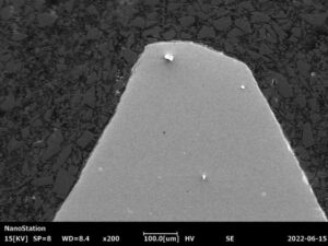
JH Technologies often receive questions from people asking us what we do and why we do it. We see many types of samples, questions, and requests from R&D to failure

Producing Memory Device Cross-Sectioning Samples Our newest JH Analytical Team member David is supporting and learning all of the functions in the lab. What better way to learn than to
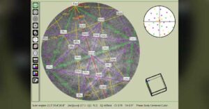
Although EBSD (Electron Backscatter Diffraction) as a technique to study the crystalline structure of materials has been around for a while now, its popularity has grown of late due to
213 Hammond Avenue Fremont, CA 94539
T 408-436-6336
F 408-436-6343
info@jhtechnologies.com